Semiconductor chip, chip stack package and manufacturing method

a semiconductor and chip technology, applied in the direction of semiconductor devices, semiconductor/solid-state device details, electrical equipment, etc., can solve the problems of too long packaging size, difficult handling, and inability to placate the appetite of consumers for increasing the functionality of electronic products

Inactive Publication Date: 2005-05-12
SAMSUNG ELECTRONICS CO LTD
View PDF6 Cites 47 Cited by
  • Summary
  • Abstract
  • Description
  • Claims
  • Application Information

AI Technical Summary

Problems solved by technology

However, as good as these devices are at reducing the size of electronics assemblies, they too have been unable to placate the appetite-of the consumer for increasing functionality of electronic products.
Since two or more packages are stacked, the size of the package increases and therefore it is very difficult to handle.
However the larger and larger chip stacks contain multiple chips which incur cooling problems.
Because the chip stack contains multiple chips, they generate more heat per unit volume, requiring greater thermal dissipation.
Moreover, this dissipation must occur now through layers of semiconductor substrate material.
However, when the chip stack package 100 includes different types of semiconductor chips 110, the conductive adhesive 160 is not easily formed due to different dimensions of the chips 110 in profile.
This causes difficulty in realizing a multi-functional stack package by using different chips.
Additionally, it is hard to efficiently inject the conductive adhesive 160 into a space between neighboring semiconductor chips 110, which results in poor electrical connection with the conductive bumps 115.

Method used


Image

  • Semiconductor chip, chip stack package and manufacturing method
  • Semiconductor chip, chip stack package and manufacturing method
  • Semiconductor chip, chip stack package and manufacturing method

Examples


Embodiment Construction

[0030] Preferred embodiments of the present invention will be described below with reference to the accompanying drawings.

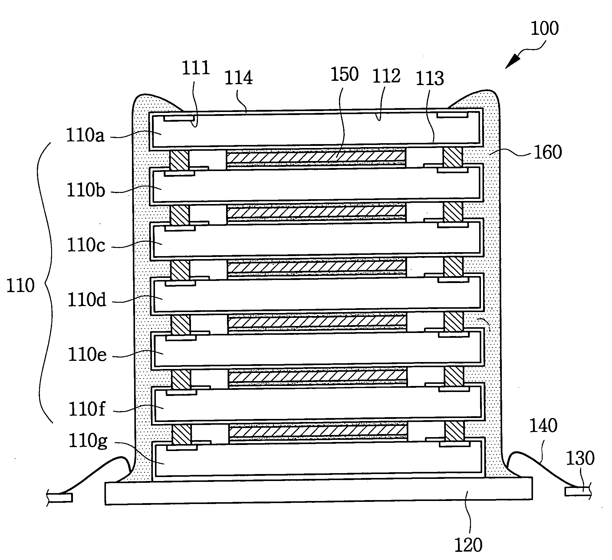
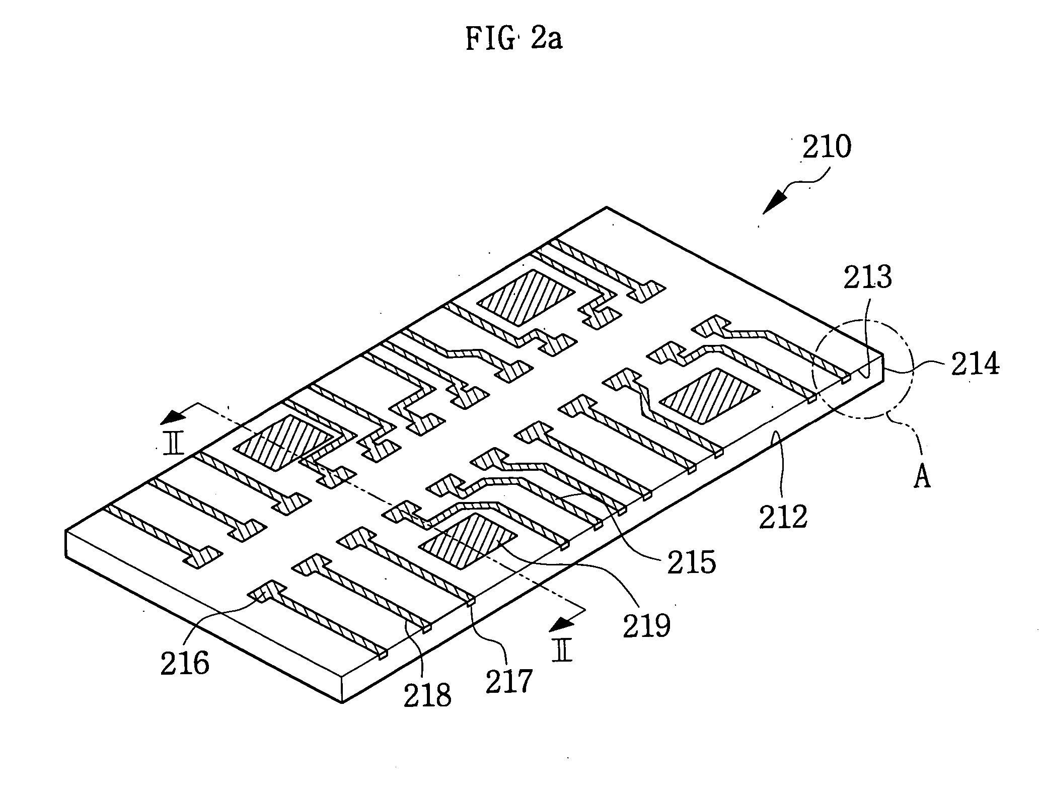
[0031]FIG. 2a is a perspective view showing a semiconductor chip 210 according to one embodiment of the present invention and FIG. 2b is a cross-sectional view taken along the line IIB-IIB of FIG. 2a. As shown in FIGS. 2a and 2b, the semiconductor chip 210 has an active surface 212 where on-chip circuits (not shown) and bonding pads 211 are formed, and a backside 213 which is the obverse to the active surface 212. The bonding pads 211 are disposed along a longer central line of the active surface 212. Therefore, the semiconductor chip 210 is a center pad type chip. The back surface 213 has bump pads 216 and connection lines 217. Each connection line 217 is connected to each bump pad 216 and extended to a side surface 215 of the semiconductor chip 210. Like the bonding pads 211, the bump pads 216 are disposed along a longer central line of the back surface 213. T...


PUM


Abstract

A semiconductor chip with conductive wiring that is routed to the edge of the substrate from the chip's backside. A plurality of such semiconductor chips are stacked and electrically connected using a wiring element that is a circuit board or conductive adhesive strips. The wiring element connects the conductive wiring of each semiconductor chip along the sides of the chips to the package substrate. A method of manufacturing the semiconductor chip includes batch manufacturing a plurality of die on a wafer with an active surface on which a plurality bonding pads are formed, and a backside which is the rear side of the active surface; forming a circuit groove on the backside; applying conductive wiring on the circuit groove using a conductive material; and separating the wafer into a plurality of semiconductor chips. A method of manufacturing the chip stack package with a plurality of such semiconductor chips having bump pads and connection pads routed to the side surface of the semiconductor chip includes stacking and bonding the bonding pad of the upper semiconductor chip on the bump pad of a lower semiconductor chip; electrically connecting the bonding pad of the lowest semiconductor chip to the substrate by bump bonding electrically connecting the wiring element to the connection pad of the semiconductor chip and the substrate; and connecting an external connection to the substrate.

Description

CROSS-REFERENCE TO RELATED APPLICATION [0001] This is a divisional application of U.S. patent Ser. No. 10 / 357,376, filed Feb. 4, 2003, which claims priority on Korean Patent Application No. 2002-6765, filed on Feb. 6, 2002, the entire contents of which are incorporated herein by reference.BACKGROUND [0002] 1. Field of the Invention [0003] The present invention relates to a chip stack package and more particularly to a semiconductor chip, a chip stack package, and method for manufacturing. [0004] 2. Description of Related Art [0005] In an atmosphere of incessant pressure to reduce the size of electronic products while maintaining and increasing their functionality, extreme attention is given to every single element of an electronic assembly. Because of growing pressure to reduce size, a whole new class of IC package, especially flip chip technique and chip-scale package techniques were introduced. However, as good as these devices are at reducing the size of electronics assemblies, t...

Claims


Application Information

Patent Timeline
Patent Type & Authority Applications(United States)
IPC IPC(8): H01L25/18H01L21/60H01L23/52H01L25/065H01L25/07
CPCH01L25/0657H01L2224/24145H01L2224/48091H01L2225/0651H01L2225/06551H01L2225/06589H01L2924/30107H01L2924/01078H01L2924/01079H01L2924/15311H01L2924/00014H01L24/24H01L24/82H01L21/60
Inventor SONG, YOUNG HEEKANG, SA YOONSON, MIN YOUNG
Owner SAMSUNG ELECTRONICS CO LTD
Why Eureka
Try Eureka