Process for manufacturing a wiring substrate

Inactive Publication Date: 2005-05-19
NGK SPARK PLUG CO LTD
View PDF2 Cites 5 Cited by
  • Summary
  • Abstract
  • Description
  • Claims
  • Application Information

AI Technical Summary

Benefits of technology

[0007] The invention contemplates to solve the aforementioned problems in the background art, and has an object to provide a wiring substrate manufacturing process which can achieve a reliable adhesion between wiring pattern layers or via conductors formed at a fine pitch and insulating resin layers adjoining the former.
[0015] According to this process, the elongation is lower than that of the insulating resin layers of the prior art. It is, therefore, possible to stably keep the state, in which the wiring pattern layers are firmly adhered to the asperities formed by the roughening step on the surfaces of the insulating resin layers.
[0017] According to this process, the Young's modulus is higher than those of the insulating resin layers of the prior art, so that influences from an external force can be suppressed from the state, in which the wiring pattern layers to be formed on the roughened surfaces of the insulating resin layers are firmly adhered.
[0018] There can be further provided, as a preferable embodiment, a wiring substrate manufacturing process, wherein at least one of the insulating resin layers (preferably, each of the insulating resin layers) has a thermal expansion coefficient in a planar (X-Y) direction: 50 ppm / ° C. or less (but excepting 0). According to this process, the thermal expansion coefficient is lower than that of the insulating resin layers of the prior art so that the influences due to the thermal change can be suppressed from the state, in which the wiring pattern layers to be formed on the surfaces of the insulating resin layers are firmly adhered.
[0020] According to this process, the wiring pattern layers are formed while being firmly adhered to the roughened surfaces of the insulating resin layers, so that they can keep the shaping and sizing precisions even they are formed to have a pattern of a fine pitch containing narrow wiring lines.

Problems solved by technology

When the wiring pattern layers of the fine pitch are to be formed or when the via conductors to connecting the overlying wiring pattern layers and the underlying wiring pattern layers are to be radially reduced, however, the current roughening treatment of the insulating resin layers and their surfaces may have an insufficient adhesion between the fine-pitched wiring pattern layers and the adjoining insulating resin layers.

Method used


Image

  • Process for manufacturing a wiring substrate
  • Process for manufacturing a wiring substrate
  • Process for manufacturing a wiring substrate

Examples


Embodiment Construction

[0033] The best mode for carrying out the invention will be described in the following. But, the invention is not limited to the range.

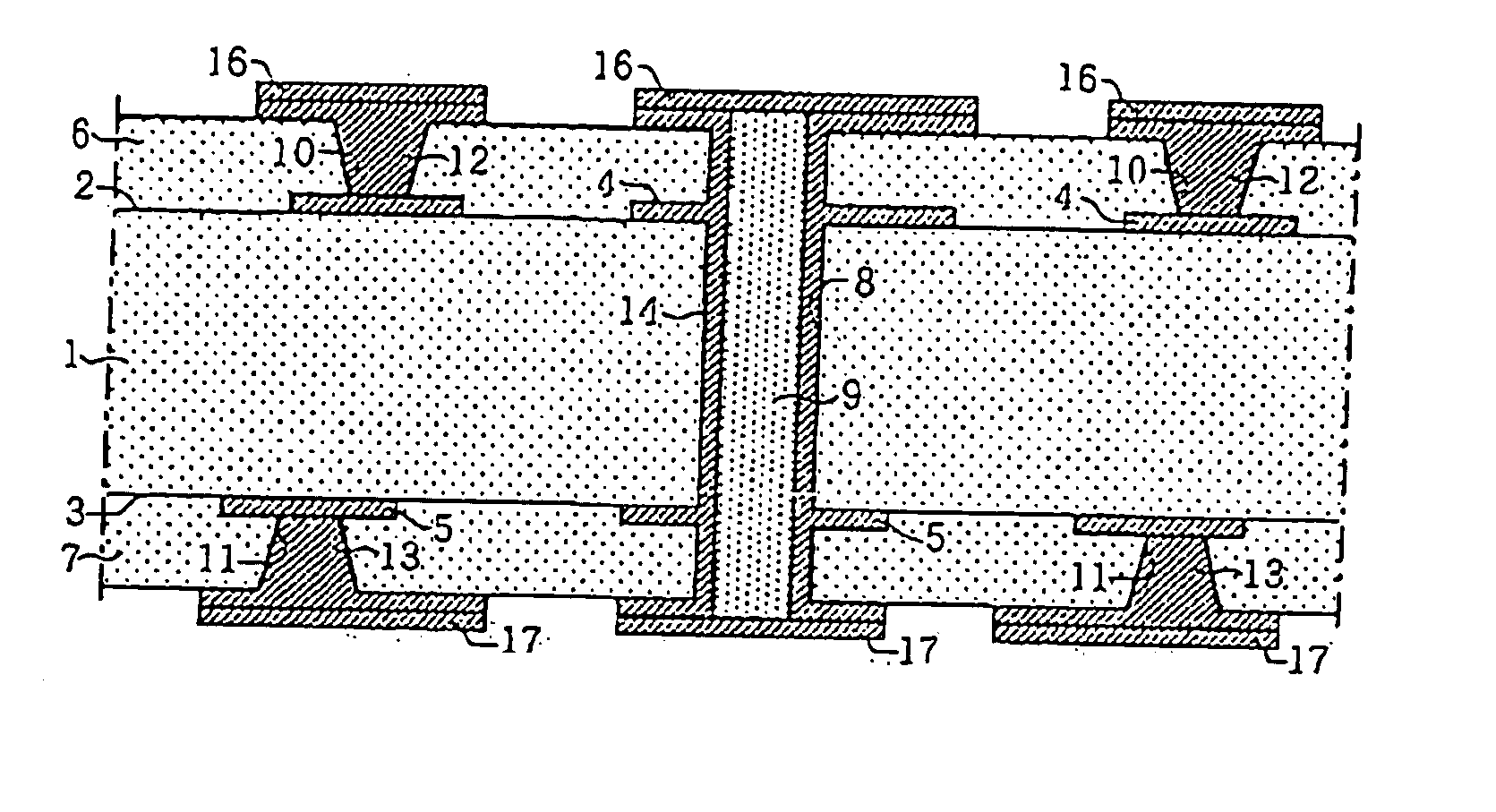
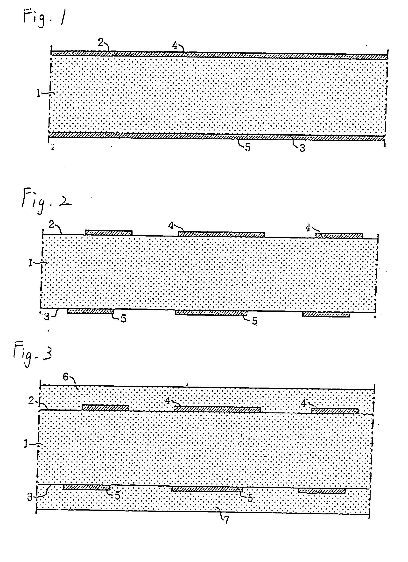
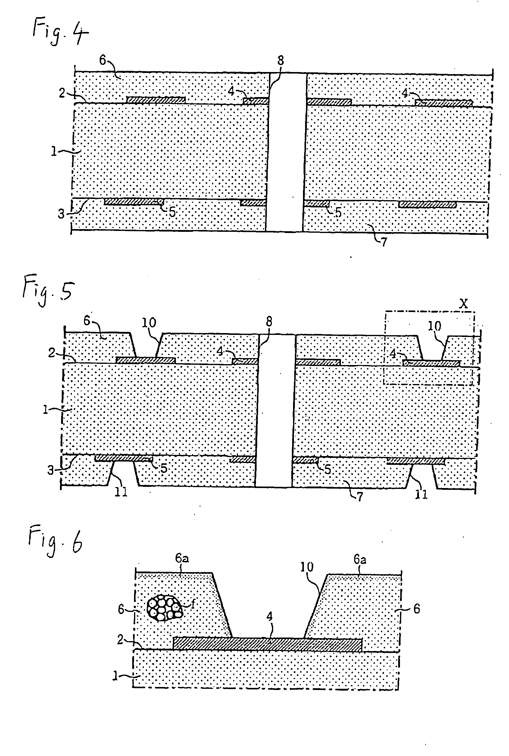
[0034]FIG. 1 is a section showing a core substrate 1 made of a bismaleimide triazine (BT) resin having a thickness of about 0.7 mm. This core substrate 1 is covered on its surface 2 and a back 3, respectively, with copper foils 4 and 5 having a thickness of about 70 μm. The not-shown photosensitive / insulating dry film is formed over those copper foils 4 and 5 and is subjected to an exposure and a development of a predetermined pattern. After this, the etching resist obtained is removed with a peeling liquid (according to the well-known subtractive method).

[0035] Here, a multi-panel having a plurality of core substrates 1 of product units may be used so that the individual core substrates 1 may be subjected to a similar treatment step (as in the following individual steps).

[0036] As a result, the cooper foils 4 and 5 become wiring layers 4 and 5 pr...


PUM

PropertyMeasurementUnit
Elongationaaaaaaaaaa
Surface roughnessaaaaaaaaaa

Abstract

A process for manufacturing a wiring substrate, comprising a roughening step of roughening surfaces of insulating resin layers, at least one of the insulating resin layers containing an epoxy resin which contains 30 to 50 wt. % of an inorganic filler of SiO2 having an average grain diameter of 1.0 to 10.0 μm, wherein the roughening step includes a roughening step of dipping in a solution of permanganic acid at 70 to 85° C. for 20 minutes or longer.

Description

FIELD OF THE INVENTION [0001] The present invention relates to a wiring substrate manufacturing method capable achieving a reliable adhesion between wiring pattern layers (e.g., built-up wiring layers) formed at a fine pitch and insulating resin layers adjoining the former. BACKGROUND OF THE INVENTION [0002] According to the trend of recent years for a high performance and a high signal-processing rate, there has been enhanced a demand for making the size of the wiring substrate smaller and the pitch of the wiring pattern layers (e.g., built-up wiring layers) finer. [0003] For example, an insulating resin layer between one wiring pattern layers and two adjoining wiring pattern layers is generally restricted by a practical limit of the section of a length×a width of 25 μm×25 μm. However, it has been demanded that the length and the width are individually 20 μm or less. [0004] In order to satisfy these demands, it As necessary not only to form the wiring pattern layer precisely in sha...

Claims


Application Information

Patent Timeline
IPC IPC(8): H05K3/38H05K3/46
CPCH05K3/381H05K3/4661Y10T29/49155H05K2203/0796Y10T29/49165H05K2201/0209
Inventor SAIKI, HAJIMESUGIMOTO, ATSUHIKO
Owner NGK SPARK PLUG CO LTD
Why Eureka
Try Eureka