Vertically aligned nanostructure scanning probe microscope tips

a scanning probe and nanostructure technology, applied in the field of nanotechnology, can solve the problems of limiting the usefulness and/or the ability to be produced in a large-scale process, the tip is very brittle and degrades easily, and the fabrication process is also serial in natur

Inactive Publication Date: 2005-05-19
UT BATTELLE LLC
View PDF8 Cites 19 Cited by
  • Summary
  • Abstract
  • Description
  • Claims
  • Application Information

AI Technical Summary

Problems solved by technology

This can generate several artifacts that obscure important features of a samples' surface structure.
While all three of these types of tips offer significant improvements over traditional etched Si tips, each suffer from several key disadvantages which limit their usefulness and / or their ability to be produced in a large scale process.
While this process can be automated with a high degree of precision it is time consuming and results in a tip that is very brittle that degrades easily.
Unfortunately, the fabrication process is also serial in nature; only a single tip can be fabricated at a time.
However, the control over the length and angle of the CNT protrusion from the Si tip is a significant problem.
In a recent work by Snow et al it was shown theoretically and experimentally that CNT tips produced in this manner do not represent a significant improvement in imaging performance over other types of high aspect ratio tips [22].
For long nanotubes, this elastic response rendered the tips unsuitable for imaging.
However, the bending response was found to be enhanced on highly textured surfaces limiting the ability to image nonplanar features.
While a method by Dai has been demonstrated for shortening CNT tips to a suitably short length for controllable imaging this reduces their production to a serial process.
It should also be noted that this offers no way to correct for variations in the alignment of the CNT with respect to the supporting Si tip.
These facts combined with the results reported by Snow clearly shows that CNT-based SPM tips are not the ideal solution to this problem.

Method used


Image

  • Vertically aligned nanostructure scanning probe microscope tips
  • Vertically aligned nanostructure scanning probe microscope tips
  • Vertically aligned nanostructure scanning probe microscope tips

Examples


example 1

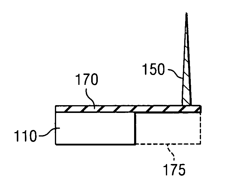
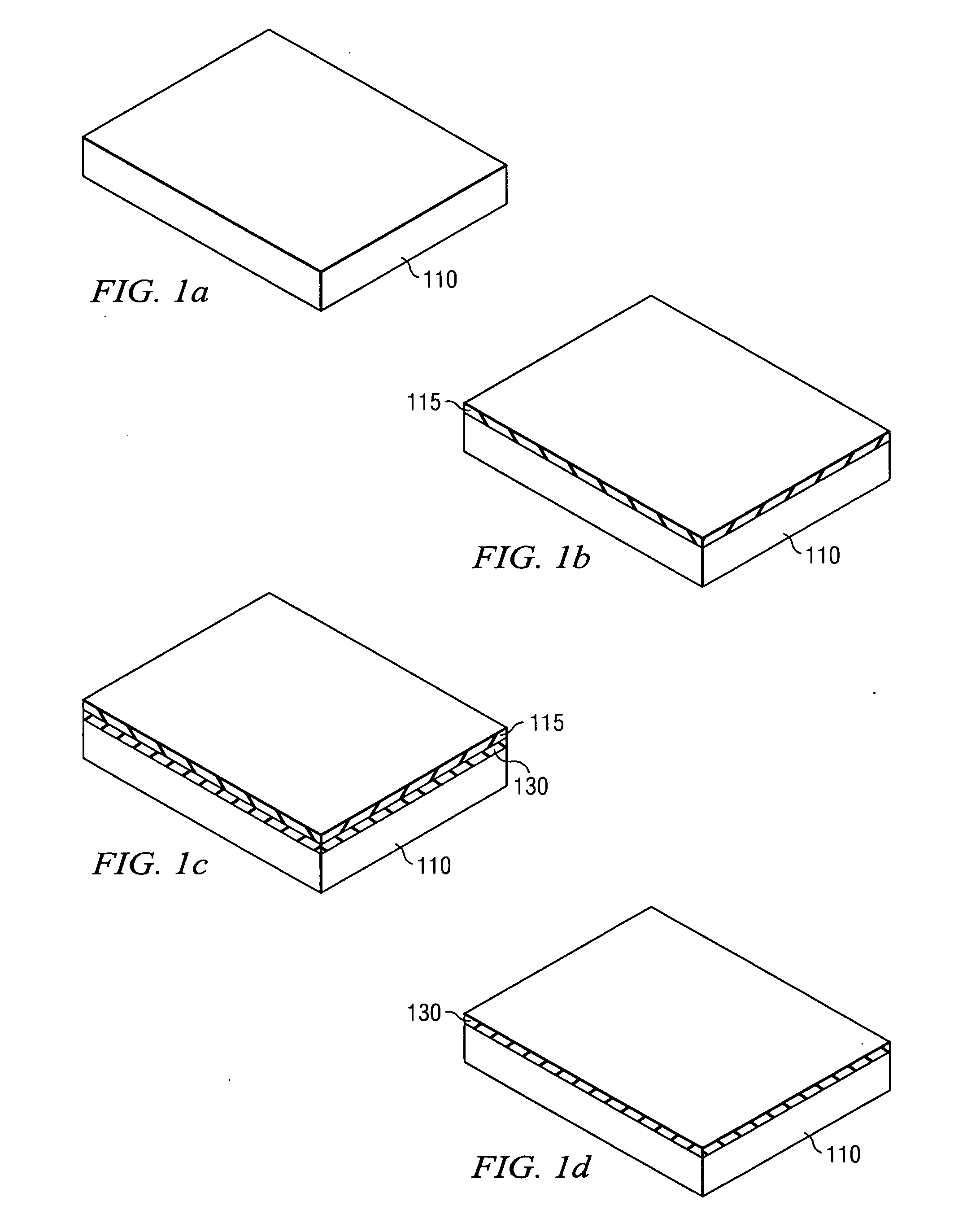
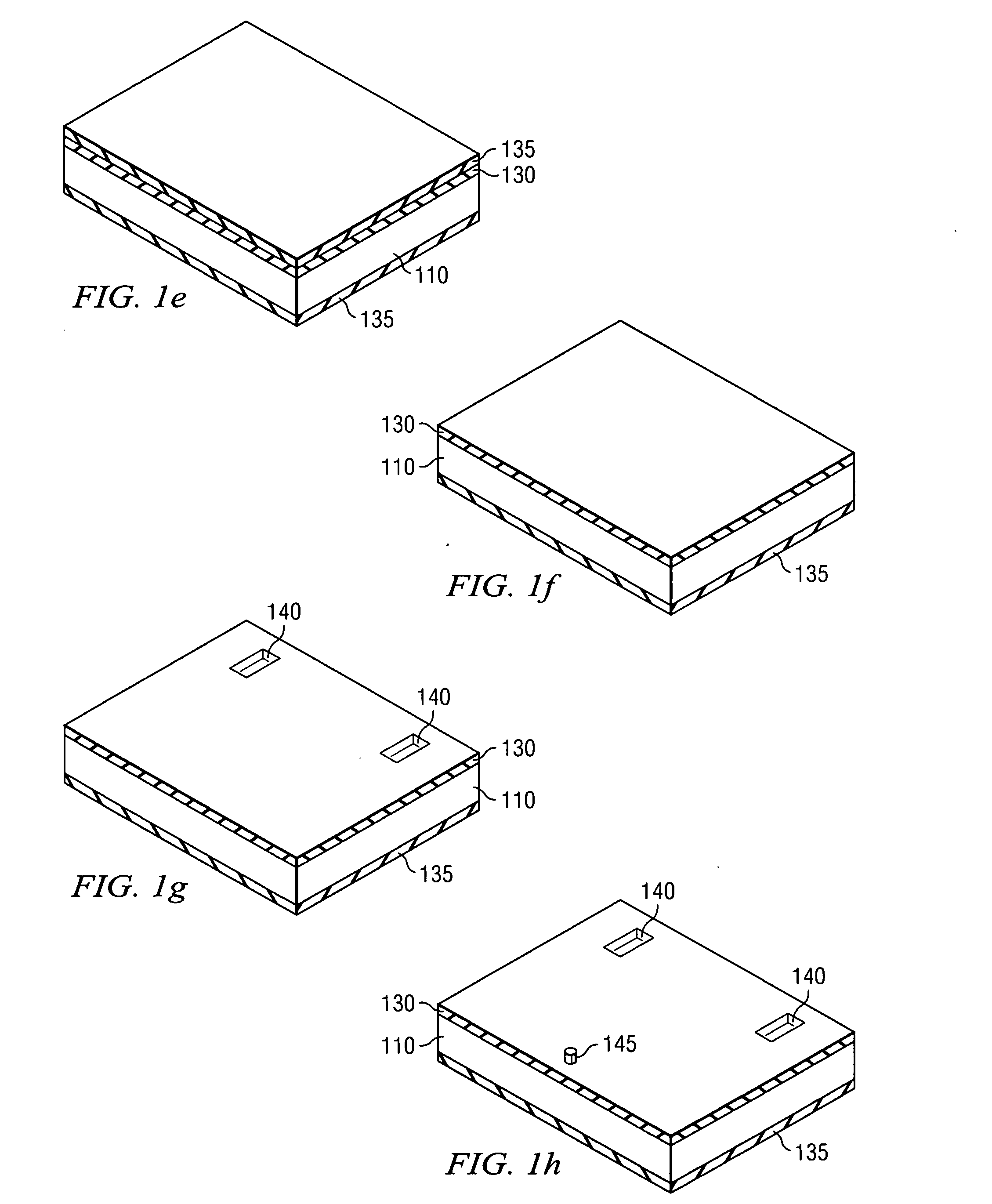
[0044] This example is a Si based process for producing high aspect ratio VACNF SPM tips on Si cantilevers using KOH for a through-wafer etch. Whole 4″ intrinsic Si double side polished wafers 110 are used as the substrate as shown in FIG. 1A. A highly doped p-type (p+) region 130 several microns deep is formed on the surface of the wafers. The depth of this layer will determine the thickness of the final cantilever structure and, ultimately, the resonant frequency of the cantilever. This doping can be accomplished using a variety of techniques. In this example, a spin-on dopant (SOD) technique based on a spin-on borosilicate glass (BSG) is depicted. After curing the SOD layer 115 at 170° C. for 1 minute (the result of this sub-process is shown in FIG. 1B), the wafers are placed in an annealing furnace operated at 1100° C. The amount of time determines the depth of the doped region 130. For a 5 μm deep p+ region, an annealing time of 5-6 hours is required (the result of this sub-pr...

example 2

[0045] This example is a Si based process for producing high aspect ratio VACNF SPM tips on Si cantilevers for electrochemical applications using KOH for the through-wafer etch. Whole 4″ intrinsic Si double side polished wafers are used as the substrate 210 as shown in FIG. 2A. A highly doped p-type (p+) region several microns deep is formed on the surface of the wafers using a spin-on dopant 215 (SOD). After curing the SOD layer 215 at 170° C. for 1 minute (the result of this sub-process is shown in FIG. 2B), the wafers are placed in an annealing furnace operated at 1100° C. The amount of time determines the depth of the doped region 230. For a 5 μm deep p+ region 230, an annealing time of 5-6 hours is required (the result of this sub-process is shown in FIG. 2C). The SOD layer is removed from the wafers using a solution of diluted HF (the result of this sub-process is shown in FIG. 2D). This process is followed by the deposition of a 200 nm thick layer of Si3N4 235 onto both side...

example 3

[0046] This example is a Si based process for producing high aspect ratio VACNF SPM tips on silicon nitride cantilevers using KOH for the through-wafer etch. Whole 4″ intrinsic Si double side polished wafers 310 are used as the substrate as shown in FIG. 3A. The wafers are placed in an LPCVD system and a layer 320 of low stress silicon nitride is deposited. This layer will form the cantilever body thus its thickness is determined by the desired resonant frequency of the cantilever structure (the result of this sub-process is shown in FIG. 3B). A 100 nm thick layer 325 of W is deposited onto the wafers. This layer 325 serves several purposes. It can be used to provide an electrical connection to the VACNF base on the completed cantilever structure. Primarily, its purpose is to prevent the surface of the wafer from charging during the direct current PECVD growth of the VACNF. If an AC discharge is used to perform the growth and no electrical contact is required to the VACNF base this...


PUM


Abstract

Methods and apparatus are described for cantilever structures that include a vertically aligned nanostructure, especially vertically aligned carbon nanofiber scanning probe microscope tips. A method includes A method, includes fabricating a cantilever structure having a vertically aligned nanostructure including: forming a doped layer at a first side of a substrate; depositing an etch mask layer on a second side of the substrate; forming a plurality of alignment marks that are coupled to the first side of the substrate; depositing a catalyst nanoparticle at a deterministic site that is coupled to the doped layer; growing the vertically aligned nanostructure at the deterministic site with the catalyst nanoparticle; depositing a first protective layer that surrounds at least a portion of the vertically aligned nanostructure; patterning the first protective layer to define an outline of a cantilever body; transferring the outline of the cantilever body from the first protective layer into the doped layer to form the cantilever body from the doped layer; depositing a second protective layer that coats at least a portion of a surface of the cantilever body; patterning the etch mask layer to define an outline of a relieved volume; transferring the outline of the relieved volume from the etch mask layer into the second side of the substrate to remove the relieved volume from the substrate, where the cantilever body is not removed.

Description

STATEMENT AS TO RIGHTS TO INVENTIONS MADE UNDER FEDERALLY-SPONSORED RESEARCH OR DEVELOPMENT [0001] This invention was made with United States Government support under prime contract No. DE-AC05-00OR22725 to UT-Battelle, L.L.C. awarded by the Department of Energy. The Government has certain rights in this invention.BACKGROUND OF THE INVENTION [0002] 1. Field of the Invention [0003] The invention relates generally to the field of nanotechnology. More particularly, the invention relates to cantilever structures that include a vertically aligned nanostructure and procedures for making a cantilever structure with a vertically aligned nanostructure. Specific embodiments of the invention are directed to scanning probe microscope tips and procedures for making scanning probe microscope tips. [0004] 2. Discussion of the Related Art [0005] Scanning probe microscopy (SPM) has become an indispensable tool for the analysis of surfaces and the exploration of general substrate morphology at the na...

Claims


Application Information

Patent Timeline
Patent Type & Authority Applications(United States)
IPC IPC(8): G01Q70/12G01Q70/16
CPCB82Y15/00G01Q70/16G01Q70/12B82Y35/00
Inventor GUILLORN, MICHAEL A.ILIC, BOJANMELECHKO, ANATOLI V.MERKULOV, VLADIMIR I.LOWNDES, DOUGLAS H.SIMPSON, MICHAEL L.
Owner UT BATTELLE LLC
Why Eureka
Try Eureka