
Three-dimensional integrated circuit with integrated heat sinks

a technology of integrated components and heat sinks, which is applied in the direction of support structure mounting, semiconductor devices, constructions, etc., can solve the problems of ic overheating and malfunction, discrete approach has limitations in wafer process technology, and achieves the effect of improving heat dissipation

Inactive Publication Date: 2005-05-19
NITTO DENKO CORP
View PDF50 Cites 114 Cited by
  • Summary
  • Abstract
  • Description
  • Claims
  • Application Information

AI Technical Summary

Benefits of technology

[0006] It is an object of the present invention to provide a three-dimensional integrated circuit with improved heat dissipation.

Problems solved by technology

The discrete approach has limitations in wafer process technology.
However, the dissipation of heat generated by the integrated components becomes a problem in three-dimensional integrated circuits.
Without proper heat dissipation, the IC may overheat and malfunction.
In a three-dimensional circuit it is difficult to provide sufficient exposure of the heat sink to the surrounds.

Method used


Image

  • Three-dimensional integrated circuit with integrated heat sinks
  • Three-dimensional integrated circuit with integrated heat sinks
  • Three-dimensional integrated circuit with integrated heat sinks

Examples


example 1

[0116] The method illustrated in FIGS. 5a -5d has been demonstrated using a one centimeter square integrated circuit chip with 41-125 μm solder bumps on 250 μm centers along one edge. This chip was mounted perpendicular to a heat sink. Prior to assembly, the first chip was coated with a bonding layer in the form of a rosin-based flux to provide enough tack to hold the chip in position during the reflow process. The assembly was then reflowed in a nitrogen-filled infrared belt furnace.

example 2

[0117] A thin-film transistor structure with top source and drain contacts was obtained using a silicon wafer with an insulating SiO2 layer. The wafer was coated with SCTCF, above which the electric contacts were deposited by conventional methods. FIG. 10 shows a schematic diagram of such an organic TFT structure with top source and drain contacts, comprising a Si wafer 55 that serves as a gate contact, a SiO2 insulating layer 56, an SCTCF 57, and gold source and drain contacts 58. The procedure of depositing contacts consisted of the following steps: (i) cutting a Si / SiO2 wafer covered with SCTCF to the required size; (ii) placing a mask (a mechanical mask was glued to the sample surface using Aquaricum silicone gel); (iii) covering the sample surface with gold. The last stage was performed using an NRC / Varian Model 3117 Thermal Evaporator equipped with a TM-350 thickness monitor (MAXTEC Inc.). The device was operated at a working pressure inside the evaporator of 10−6-10−7 Torr an...


PUM


Abstract

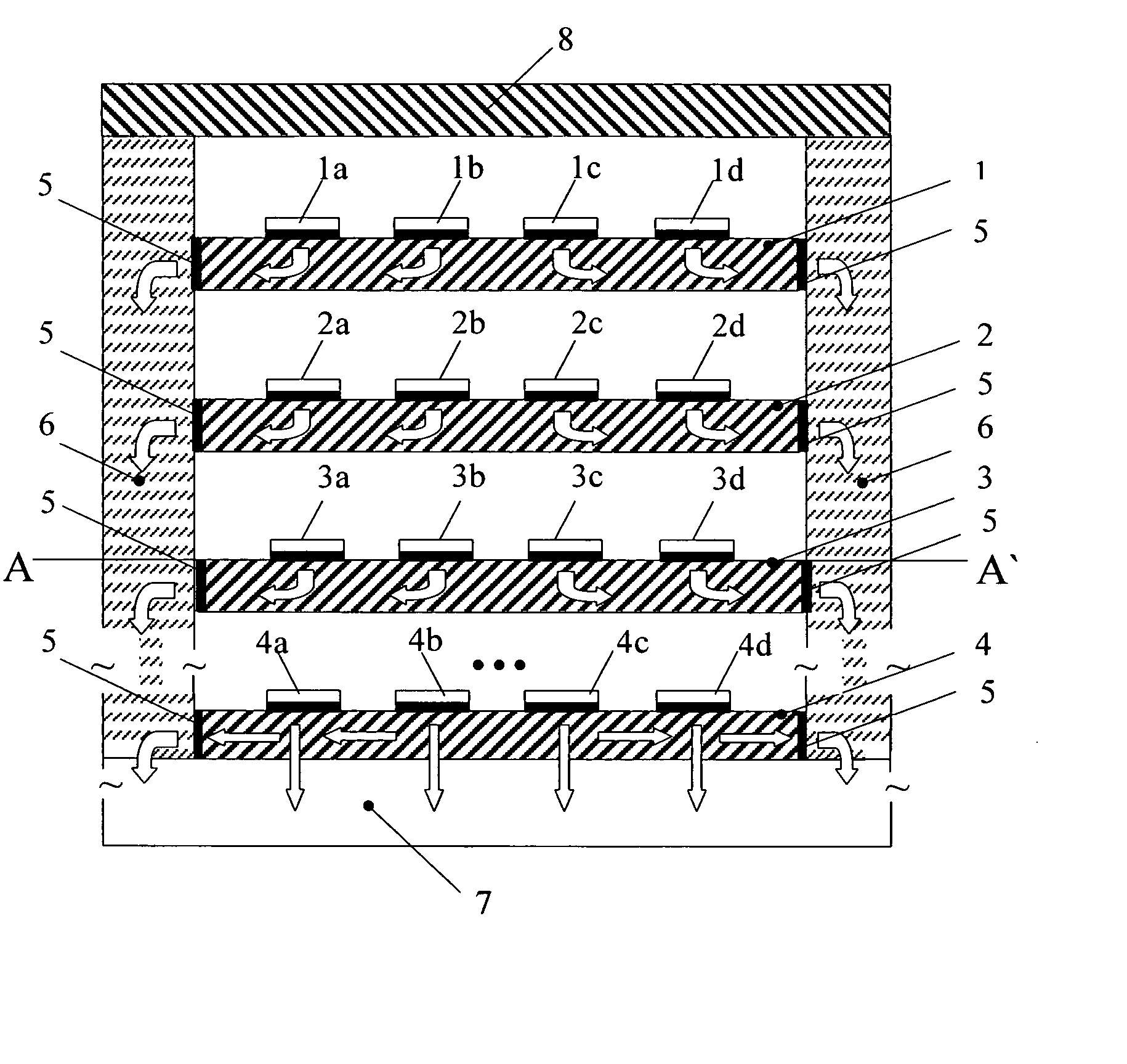
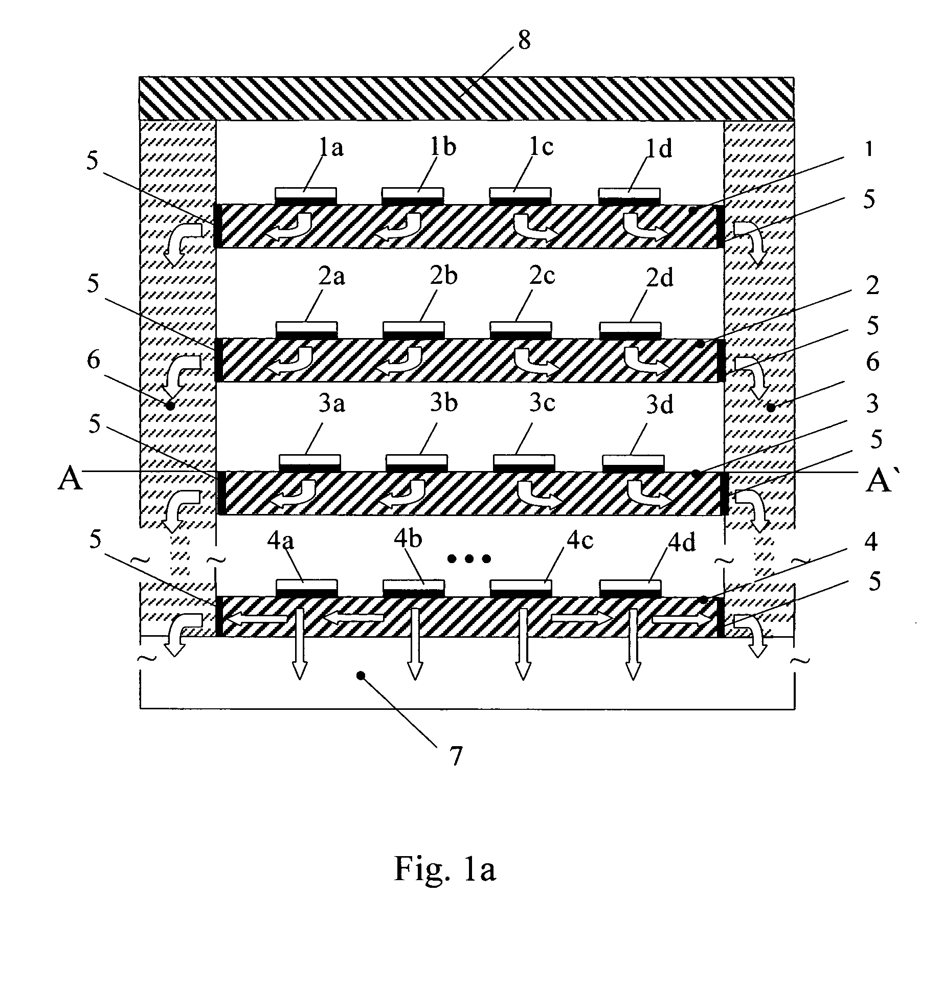
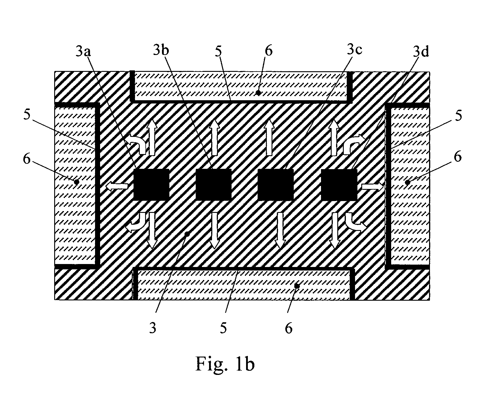
The present invention is directed to a three-dimensional semiconducting integrated circuit incorporating an integrated heat-sink dissipating heat produced by the semiconductor device mounted thereon.

Description

RELATED APPLICATION [0001] This application claims the benefit of, and priority to, of U.S. provisional patent application Ser. No. 60 / 152,256 filed on Oct. 17, 2003, entitled “Three-Dimensional Integrated Circuit with Integrated Heat Sinks”, the entire disclosure of which is incorporated herein by reference.FIELD OF THE INVENTION [0002] The present invention relates to a three-dimensional integrated circuit incorporating an integrated heat sink for dissipating heat produced by the integrated semiconductor devices mounted thereon. BACKGROUND OF THE INVENTION [0003] Conventional ICs are formed on the surface of a silicon substrate. A high integration is achieved through enlarging the chip area and employing a discrete approach, which implies making each individual element small and each wiring fine. The discrete approach has limitations in wafer process technology. Accordingly, three-dimensional ICs have been proposed. [0004] However, the dissipation of heat generated by the integrat...

Claims


Application Information

Patent Timeline
Patent Type & Authority Applications(United States)
IPC IPC(8): H01L25/065H05K7/14
CPCH01L25/0652H01L25/0657H01L2225/06517H01L2225/06541H01L2225/06551H01L2924/0002H01L2225/06589H01L2924/00H01L2224/16105H01L24/13H01L24/16H01L24/81H01L2224/0401H01L2224/13023H01L2224/16057H01L2224/16238H01L2224/81815H01L2224/05568H01L2224/16108
Inventor LAZAREV, PAVEL I.
Owner NITTO DENKO CORP
Learn More