Electroplated CoWP composite structures as copper barrier layers

a composite structure and cobalt technology, applied in the direction of layered products, semiconductor/solid-state device details, chemistry apparatus and processes, etc., can solve the problems of insufficient technology for deposition of single-crystalline thin films, difficult control, and many attempts by skilled researchers to obtain effective amorphous materials

Active Publication Date: 2005-05-19
TAIWAN SEMICON MFG CO LTD
View PDF9 Cites 48 Cited by
  • Summary
  • Abstract
  • Description
  • Claims
  • Application Information

AI Technical Summary

Problems solved by technology

PVD or CVD capping materials are not selective and require a CMP or etching step to remove the film from the dielectric.
However, electroless processes typically require a seeding scheme (to start the nucleation of the deposit) as well as high plating temperatures, and are difficult to control especially for films less than 300 Å thick.
However, deposition of single crystalline thin films can not yet be technologically realized.
Although amorphous materials are, in principle, very attractive for use as capping materials, many attempts by skilled researchers to obtain effective amorphous materials have failed.
However, as emphasized by Kohn, electroless deposited CoWP films are limited to about 8 to 10 atomic percent phosphorous.

Method used


Image

  • Electroplated CoWP composite structures as copper barrier layers
  • Electroplated CoWP composite structures as copper barrier layers
  • Electroplated CoWP composite structures as copper barrier layers

Examples


examples

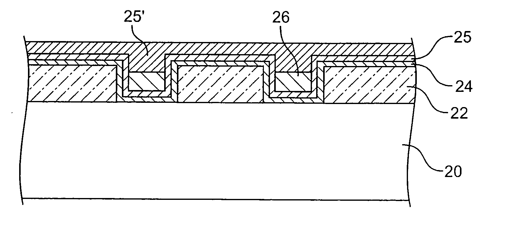
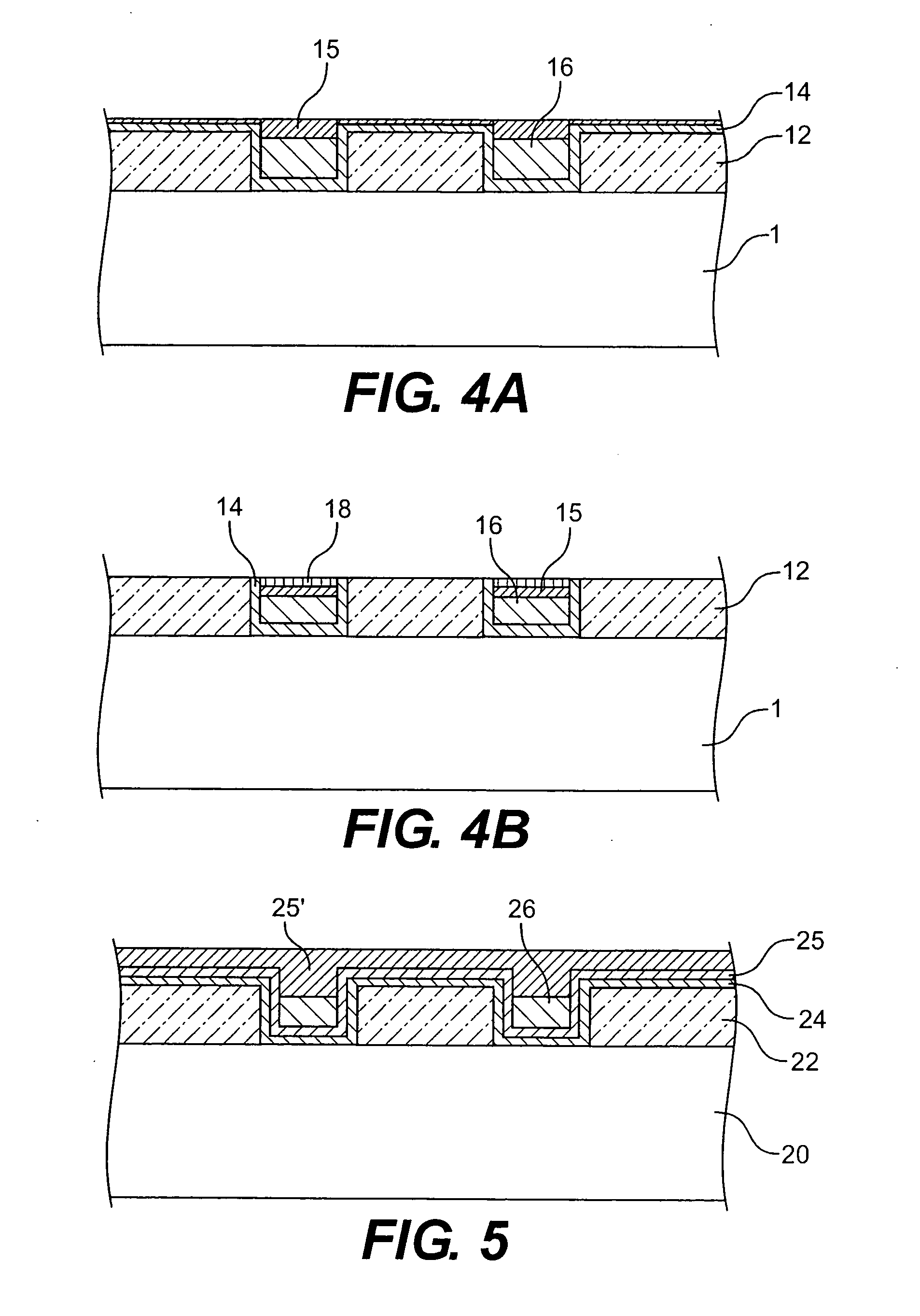
[0050] The CoWP films of the invention were electroplated on a composite structure substrate comprising a blanket p-Si with a TaN / Ta barrier layer, a PVD copper seed layer and an electroplated copper layer of dimension 4×4 cm. The electroplating process included a modified rotating disc electrode controlled by a power supply, which operated with a Pine Instruments system. The modified rotating disc electrode included a metal shaft screwed into a plug which contained a metal top surface and Teflon sample holder with a recessed insert. Four contact pins placed through the plug held the sample in place in the insert and provided the path for the current.

[0051] The agitation of the samples was between 50 and 200 rpm and the current density was varied between 5 and 10 mA / cm2. The pH of the electroplating solutions was varied from 4 to 9 by adding sulfuric acid or sodium hydroxide to the solutions as necessary. The temperature of the solutions was controlled by a double jacketed cell and...

example a

[0059] CoWP film A prepared from bath solution A was deposited at 40° C., 100 rpms, and 6.3 mA / cm2. The deposited film was annealed to 400° C. for 4 hours in forming gas (5% H2 in N2) and showed no crystallinity. The CoWP film A had an atomic percent concentration of 77.6 / 5.9 / 16.5 of Co, W and P, respectively, by RBS analysis, and a film thickness of about 160 nm.

[0060] The x-ray diffraction spectrum of Example A is provided in FIG. 7A. The spectrum was obtained following a 400° C. anneal for 4 hours. A slow run data set (shown as inset) from 38 2θ to 42.6 2θ indicates virtual absence of a crystalline Co2P peak at ca. 41° 20.

example b

[0061] CoWP film B prepared from bath solution B was deposited at 50° C., 100 rpms, and 5 mA / cm2. The deposited film was annealed at 400° C. for about 30 minutes in forming gas. At the end of the 30 minute anneal the film exhibited no crystalline structure by XRD. Following an additional anneal of 4 hours under the same conditions, CoWP film B exhibited very little crystalline structure by XRD (a single, weak intensity Co2P (121) peak; no other phases identified). The CoWP film B had an atomic percent concentration of 70 / 6 / 24 of Co, W and P respectively, and a thickness of about 100 nm.


PUM

PropertyMeasurementUnit
thicknessaaaaaaaaaa
thicknessaaaaaaaaaa
thicknessaaaaaaaaaa

Abstract

A composite material comprising a layer containing copper, and an electrodeposited CoWP film on the copper layer. The CoWP film contains from 11 atom percent to 25 atom percent phosphorus and has a thickness from 5 nm to 200 nm. The invention is also directed to a method of making an interconnect structure comprising: providing a trench or via within a dielectric material, and a conducting metal containing copper within the trench or the via; and forming a CoWP film by electrodeposition on the copper layer. The CoWP film contains from 10 atom percent to 25 atom percent phosphorus and has a thickness from 5 nm to 200 nm. The invention is also directed to a interconnect structure comprising a dielectric layer in contact with a metal layer; an electrodeposited CoWP film on the metal layer, and a copper layer on the CoWP film.

Description

FIELD OF THE INVENTION [0001] The invention is directed to electroplated cobalt tungsten phosphide-copper composite structures. The electroplated cobalt tungsten phosphide film, hereafter CoWP film, present in the composite structures can be used as a barrier layer for copper interconnect structures in a semiconductor device. BACKGROUND OF THE INVENTION [0002] Aluminum-copper and related alloys were once the preferred alloys for forming interconnect structures in electronic devices such as integrated circuit chips. However, the present demands of the microelectronic industry for increased density and high performance (speed and efficiency) requires that the interconnect structures consist of pure or nearly pure copper. Performance is improved because the resistivity of copper and certain copper alloys is much lower than the resistivity of aluminum-copper. Also, narrow interconnect structures (lines) can be used, thus providing higher wiring densities. [0003] Typically, copper interc...

Claims


Application Information

Patent Timeline
Patent Type & Authority Applications(United States)
IPC IPC(8): B32B15/04C25D3/56C25D9/08H01L21/288H01L21/44H01L21/768H01L23/48H01L23/52H01L23/532H01L29/40
CPCC25D9/08H01L21/2885H01L21/76838H01L21/76843H01L21/76846H01L21/76849H01L2924/0002H01L21/76877H01L23/53238H01L2924/00H01L2224/05007
Inventor CABRAL, CYRIL JR.CHIRAS, STEFANIE R.COOPER, EMANUEL I.DELIGIANNI, HARIKLIAKELLOCK, ANDREW J.RUBINO, JUDITH M.TSAI, ROGER Y.
Owner TAIWAN SEMICON MFG CO LTD
Why Eureka
Try Eureka