Electrostatic discharge testers for undistorted human-body-model and machine-model characteristics

a technology of electrostatic discharge and testers, applied in the field of electronic systems and semiconductor devices, can solve the problems of inability to keep up with the increased parasitics of high pin count sockets and boards used to test the ics, severe damage to the integrated circuit (ics), and thermal runaway in the device, and achieve the effect of easy adoption

Active Publication Date: 2005-05-19
TEXAS INSTR INC
View PDF2 Cites 5 Cited by
  • Summary
  • Abstract
  • Description
  • Claims
  • Application Information

AI Technical Summary

Benefits of technology

[0011] A technical advantage of the invention is its simplicity so that it can easily be adopted into any ESD tester and integrated circuit testing methodology.
[0012] The technical advances represented by the invention, as well as the aspects thereof, will become apparent from the following description of the preferred embodiments of the invention, when considered in conjunction with the accompanying drawings and the novel features set forth in the appended claims.

Problems solved by technology

Integrated circuits (ICs) may be severely damaged by electrostatic discharge (ESD) events.
Second breakdown is a phenomenon that induces thermal runaway in he device wherever the reduction of the impact ionization current is offset by the thermal generation of carriers.
ESD testers, however, have not kept up with the increased parasitics of the high pin count sockets and boards that are used to test the ICs.
Obviously, the testers have to be trustworthy in order to deliver undistorted pulses to evaluate the ESD robustness of semiconductor products, but the testers have been found to be severely lacking unambiguous testing performance.
Consequently, the test results have been found to be misleading with respect to the ESD evaluation of semiconductor products.
Such false data may not only lead to wasted resources, lost time, and customer misunderstanding, but also lead to situations where true versus false ESD levels are not determined properly.

Method used


Image

  • Electrostatic discharge testers for undistorted human-body-model and machine-model characteristics
  • Electrostatic discharge testers for undistorted human-body-model and machine-model characteristics
  • Electrostatic discharge testers for undistorted human-body-model and machine-model characteristics

Examples


Embodiment Construction

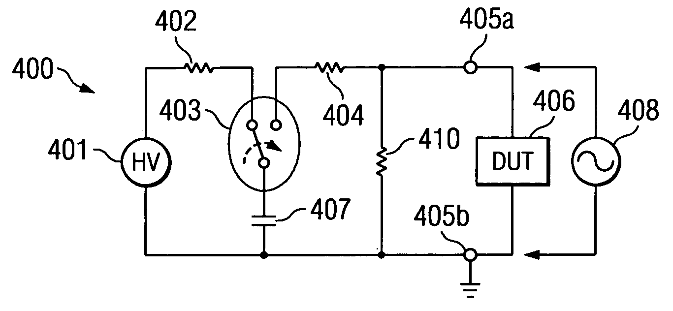
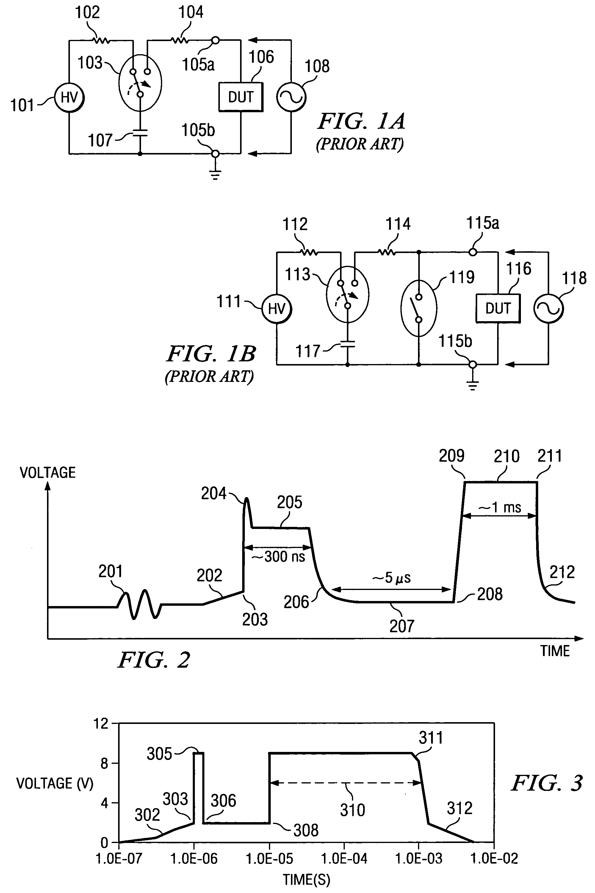
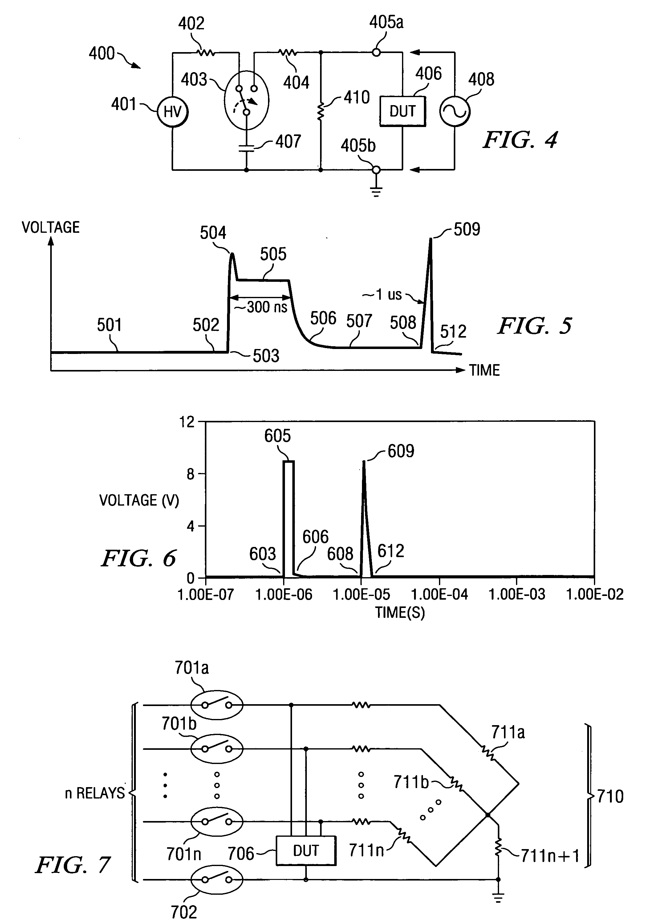
[0021] The impact of the invention can be most easily appreciated when compared with the shortcomings of the known technology. FIG. 1A depicts a schematic and simplified circuit diagram of the ESD testers as they are routinely employed by known technology to test semiconductor product from various technologies according to the requirements of the Human Body Model (HBM). FIG. 1B depicts a similarly schematic and simplified circuit diagram of ESD testers for testing semiconductor products according to the requirements of the Machine Model (MM). The high voltage generator 101 delivers about 8 kV (up to 15 kV) and is connected, through first resistor 102 of about 1 to 5 MΩ, to the on / off switch relay 103. Typically, commercial testers employ relays 103 which operate in a partially ionized ambient and are thus inclined to arc; in the case of arcing, the high voltage supply 101 is able to provide a leakage current.

[0022] Relay 103 is connected, through a second resistor 104 of about 1.5 ...


PUM


Abstract

An equipment (400) for testing semiconductor device performance under high energy pulse conditions, which comprises a high voltage generator (401) and an on/off switch relay (403). The relay is resistively connected by a first resistor (402) to the generator and by a second resistor (404) to the socket (405a) for the device-under-test (406); the relay is operable in a partially ionized ambient. A capacitor (407) is connected to the relay, to the generator, and to the device, and is operable to discharge high energy pulses through the device. A third resistor (410) is in parallel with the capacitor and the device, and is operable to suppress spurious pulses generated by the relay. This third resistor has a value between about 1 kΩ and 1 MΩ, preferably about 10 kΩ, several orders of magnitude greater than the on-resistance of the device-under-test.

Description

FIELD OF THE INVENTION [0001] The present invention is related in general to the field of electronic systems and semiconductor devices and more specifically to method and equipment of testing semiconductor devices based to the human-body model and the machine model. DESCRIPTION OF THE RELATED ART [0002] Integrated circuits (ICs) may be severely damaged by electrostatic discharge (ESD) events. A major source of ESD exposure to ICs is from the human body (described by the “Human Body Model”, HBM); the discharge of the human body generates peak currents of several amperes to the IC for about 100 ns. A second source of ESD is from metallic objects (described by the “Machine model”, MM); it can generate transients with significantly higher rise times and current levels than the HBM ESD source. A third source is described by the “charged device model” (CDM), in which the IC itself becomes charged and discharges to ground in rise times less than 500 ps. [0003] ESD phenomena in ICs are grow...

Claims


Application Information

Patent Timeline
Patent Type & Authority Applications(United States)
IPC IPC(8): G01R31/00G01R31/12G01R31/14
CPCG01R31/002G01R31/14G01R31/129
Inventor DUVVURY, CHARVAKAKUNZ, JOHN E. JR.STEINHOFF, ROBERT M.
Owner TEXAS INSTR INC
Why Eureka
Try Eureka