Lithographic apparatus and device manufacturing method
- Summary
- Abstract
- Description
- Claims
- Application Information
AI Technical Summary
Benefits of technology
Problems solved by technology
Method used
Image
Examples
Embodiment Construction
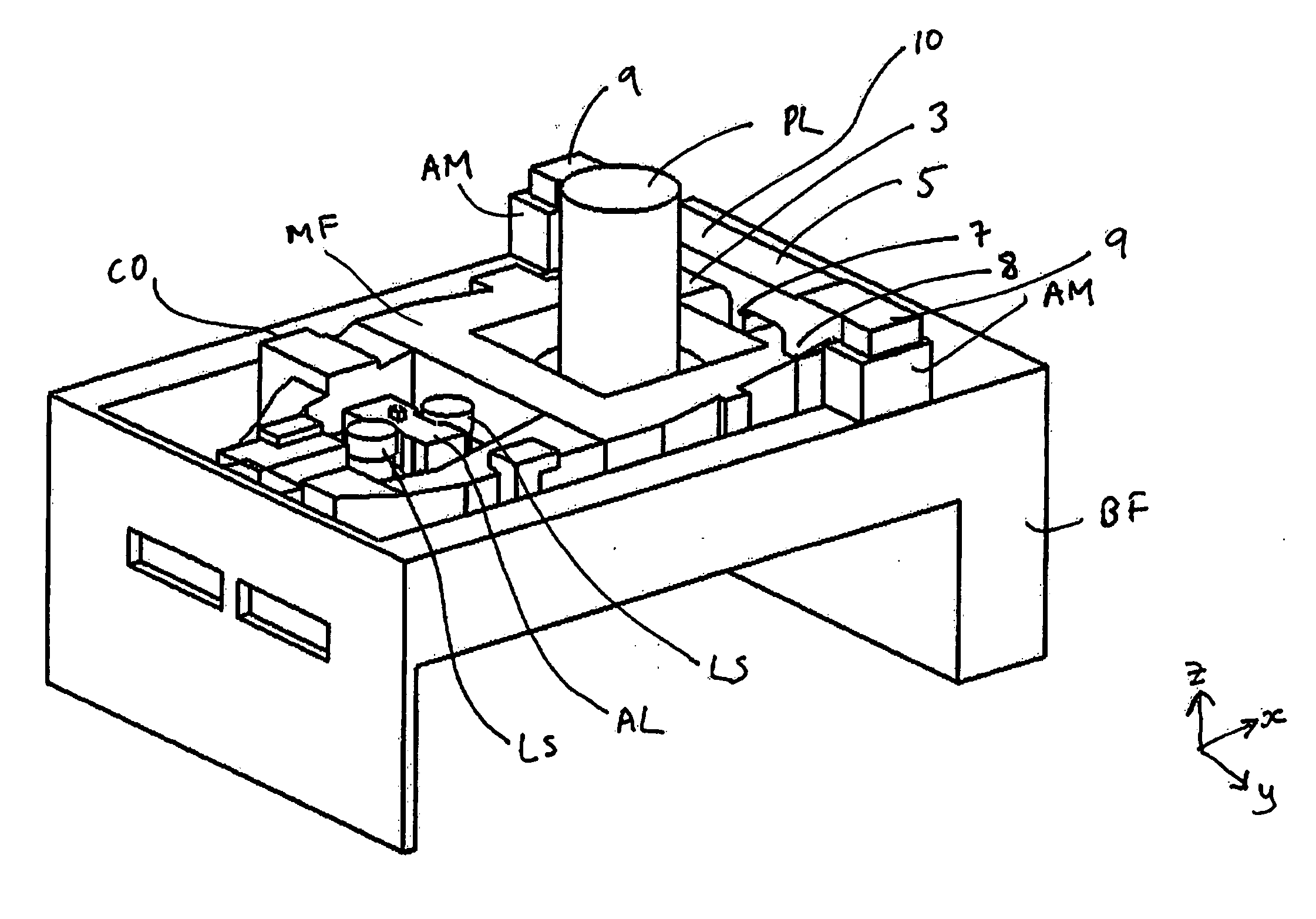
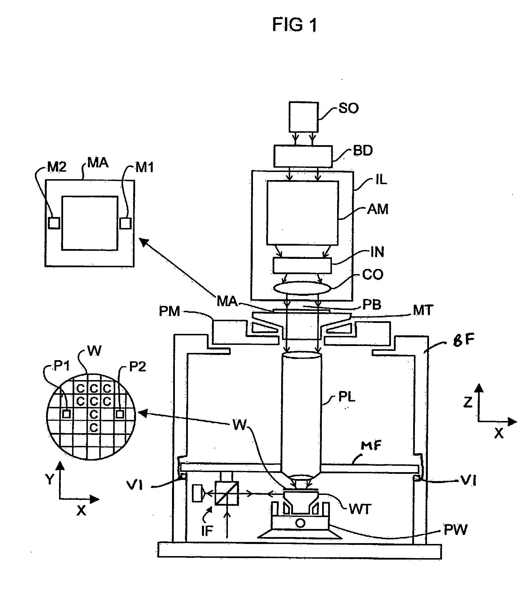
[0039]FIG. 1 schematically depicts a lithographic apparatus according to a particular embodiment of the invention. The apparatus comprises: an illumination system (illuminator) IL for providing a projection beam PB of radiation (e.g. UV radiation or EUV radiation); a first support structure (e.g. a mask table) MT for supporting a patterning structure (e.g. a mask) MA and connected to a first positioning device PM for accurately positioning the patterning structure with respect to item PL; a substrate table (e.g. a wafer table) WT for holding a substrate (e.g. a resist coated wafer) W and connected to a second positioning device PW for accurately positioning the substrate with respect to item PL; and a projection system (e.g. a refractive projection lens) PL for imaging a pattern imparted to the projection beam PB by the patterning structure MA onto a target portion C (e.g. comprising one or more dies) of the substrate W. The term “substrate table” as used herein can also be consider...
PUM
 Abstract
Description
Claims
Application Information
 - R&D
- Intellectual Property
- Life Sciences
- Materials
- Tech Scout
- Unparalleled Data Quality
- Higher Quality Content
- 60% Fewer Hallucinations
Browse by: Latest US Patents, China's latest patents, Technical Efficacy Thesaurus, Application Domain, Technology Topic, Popular Technical Reports.
© 2025 PatSnap. All rights reserved.Legal|Privacy policy|Modern Slavery Act Transparency Statement|Sitemap|About US| Contact US: help@patsnap.com


