Optical device mounted substrate assembly

Active Publication Date: 2005-05-19
NGK SPARK PLUG CO LTD
View PDF5 Cites 78 Cited by
  • Summary
  • Abstract
  • Description
  • Claims
  • Application Information

AI Technical Summary

Benefits of technology

[0031] In the alignment hole forming step, the alignment hole is formed in the optical waveguide or the optical fiber connector. Here, known perforating techniques can be used in the alignment hole forming step. Specific examples are drilling, punching, etching, and laser beam machining. However, in view of low costs, mechanical machining such as drilling and punching are preferable. Furthermore, more preferably, drilling or machining conducted here is precision drilling with a precision drill. This is because the optical axis alignment can be conducted highly accurately when the alignment hole is formed by these methods. Moreover, the alignment hole may be a through hole opened through the front and back sides of the optical waveguide or the optical fiber connector and a non-through hole opened only in the back side. Besides, it will do to make fine adjustment

Problems solved by technology

For this reason, alignment accuracy is insufficient, and a shift or movement of the optical axes of the optical device relative to the optical axes of the optical waveguide tends to be caused, thus likely causing an optical transmission loss.
Therefore, such techniques are considered incapable of sufficiently meeting a demand for realization of high speed and high density optical communicated expected in future.
Moreover, in the case where the circuit board is a resin substrate, heat radiation or dissipation of the optical device and an operation circuit thereof is deteriorated.
Therefore, stable operating characteristics cannot be obtained in this case.
In addition, in ca

Method used


Image

  • Optical device mounted substrate assembly
  • Optical device mounted substrate assembly
  • Optical device mounted substrate assembly

Examples


first embodiment

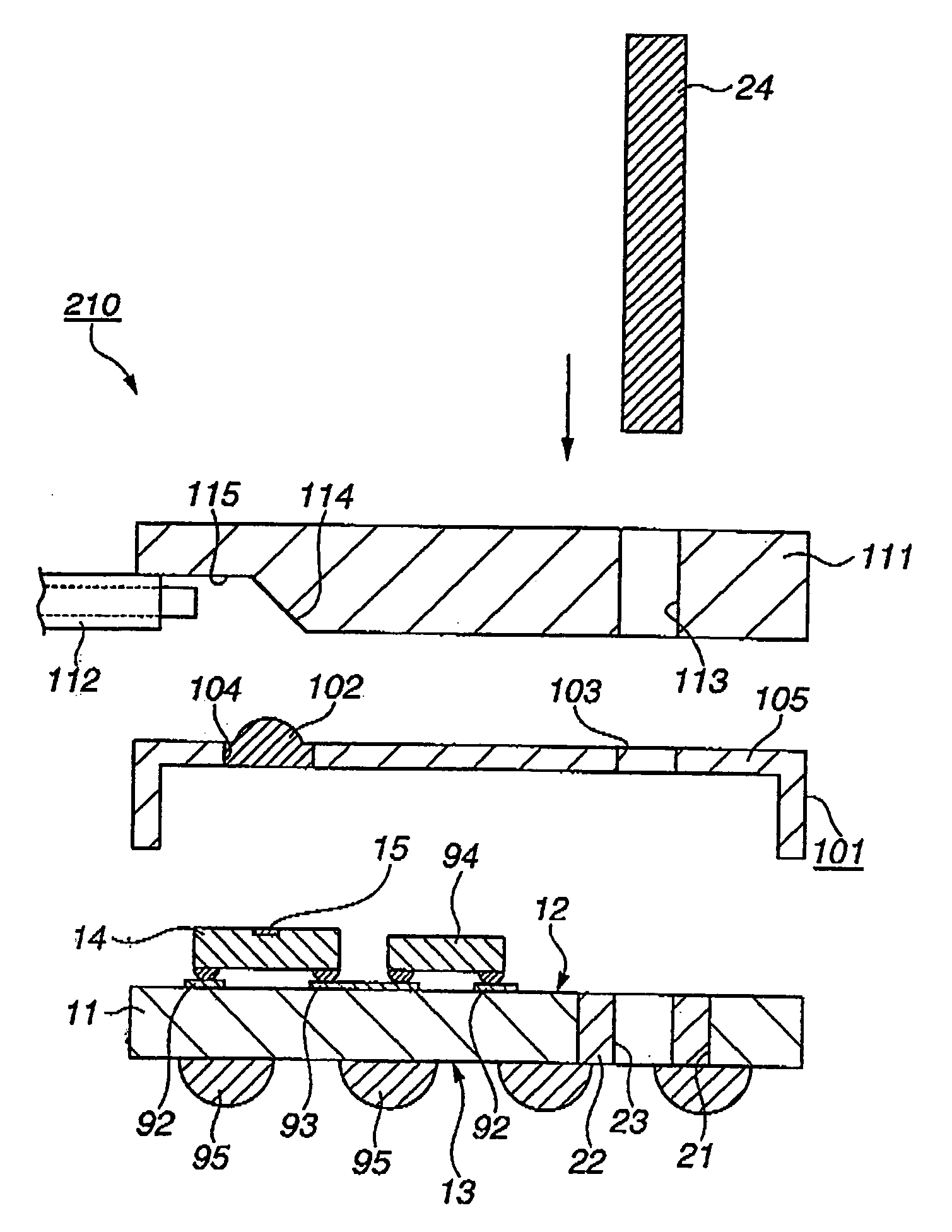
[0086] Hereinafter, an optical waveguide equipped optical device mounted substrate assembly (substrate assembly for supporting an optical component equipped with another optical component) 10 according to a first embodiment of the present invention will be described in detail with reference to FIG. 1 to 13.

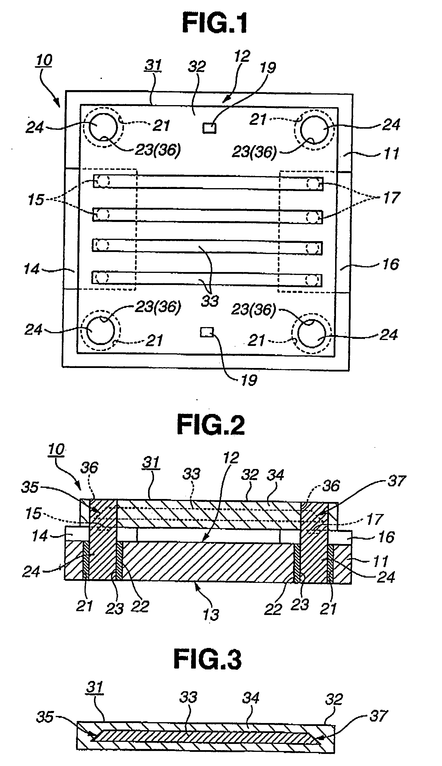
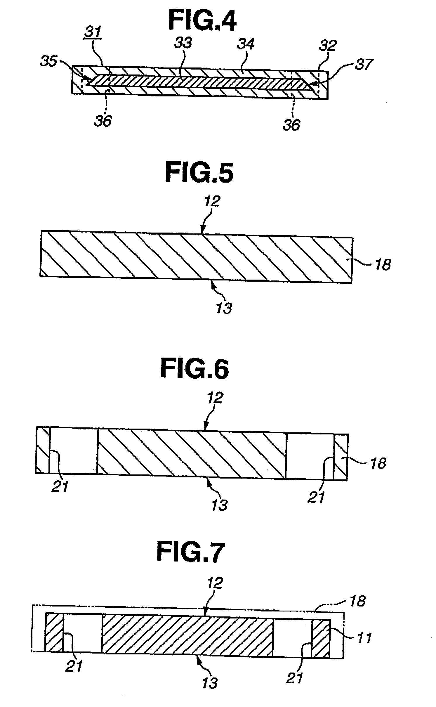
[0087] As shown in FIGS. 1 and 2, a ceramic substrate 11 configuring the optical device mounted substrate assembly 10 of the embodiment is a nearly rectangular plate member having a top surface 12 (front surface) and an under surface 13. This ceramic substrate 11 is a so-called multilayer circuit board having the top surface 12 (front surface), the under surface 13, and metal interconnect layers, not shown. The ceramic substrate 11 also has via hole conductors (omitted in the drawing), and the metal interconnect layers in different layers are in interlayer connection through the via hole conductors.

[0088] In FIG. 2, a VCSEL 14 (optical device), which is one kind of optical devic...

second embodiment

[0111] Next, an optical waveguide equipped optical device mounted substrate assembly (substrate assembly for supporting an optical component equipped with another optical component) 10 according to a second embodiment of the present invention will be described. The embodiment is different from the first embodiment only in that the composition of a resin layer 22 is varied from that of the first embodiment.

[0112] In the resin layer forming step, 5 parts by weight of a curing agent (2P4MZ-CN made by Shikoku Corp.), 600 parts by weight of a copper filler (SRF-Cu-10 made by Nippon Atomized Metal Powders Corporation), an anti-foaming agent (BERENOL S-4 made by SAN NOPCO LIMITED), and a thickening agent (RY200 made by Nippon Aerosil Co., Ltd.) are first mixed to 100 parts by weight of an epoxy resin (Epikote 828 made by JER Co., Ltd.). The mixture is kneaded with triple rolls to form a resin material for forming the resin layer 22. That is, an uncured resin material containing an inorgan...

third embodiment

[0114] FIGS. 14 to 16 depict an optical fiber connector equipped optical device mounted substrate assembly 110 of a third embodiment that the invention is made concrete. Here, the points different from the first embodiment will be described, but the same points as the first embodiment are only designated the same component numbers.

[0115] As shown in FIGS. 14 and 15, an optical fiber connector 52 of the optical fiber connector equipped optical device mounted substrate assembly 110 is a so-called MT connector disposed at the tip end of an optical fiber 51 of a multicore structure (four cores in FIG. 14). The end face (that is, the end of each of cores 33) of the optical fiber 51 is exposed in the lower end face of the optical fiber connector 52. A pair of alignment holes 54 opened in the lower end face is disposed at both ends in the lower end face of the optical fiber connector 52. Then, guide pins 24 of a ceramic substrate 11 are fitted in the alignment holes 54. Consequently, the ...


PUM

PropertyMeasurementUnit
Diameteraaaaaaaaaa
Transmissionaaaaaaaaaa
Thermal conductivityaaaaaaaaaa

Abstract

An optical device mounted substrate assembly includes a ceramic substrate having a first recess, an optical device mounted on the ceramic substrate and having one of a light emitting portion and a light receiving portion, the optical device being to be optically connected to one of an optical waveguide and an optical fiber connector in way as to align optical axes of the optical wave guide or the optical fiber connector with each other, a resin layer disposed in the first recess and having a second recess smaller in diameter than the first recess, and an alignment guide member fitted in the second recess and having a protruded portion protruding from a front surface of the ceramic substrate and fittingly engageable in an alignment hole of one of the optical waveguide and the optical fiber connector. A fabrication method of such a substrate assembly is also provided.

Description

BACKGROUND OF THE INVENTION [0001] The present invention relates to an improvement in or relating to an optical device mounted substrate assembly. More specifically, the present invention relates to an optical device mounted substrate assembly (i.e., an assembly of a substrate and an optical device) and a fabrication method thereof, an optical waveguide equipped optical device mounted substrate assembly (i.e., an assembly of a substrate and an optical device equipped with an optical waveguide) and a fabrication method thereof, an optical fiber connector equipped optical device mounted substrate assembly (i.e., an assembly of a substrate and an optical device equipped with an optical fiber connector and a fabrication method thereof, and an optical component equipped optical device mounted substrate assembly (i.e. an assembly of a substrate and an optical device equipped with an optical component). [0002] In recent years, with the development of information communication techniques re...

Claims


Application Information

Patent Timeline
IPC IPC(8): G02B6/42
CPCG02B6/4206G02B6/4236G02B6/4231G02B6/4214H01L2224/16225H01L2924/15311
Inventor OONO, TAKESHITAKADA, TOSHIKATSUONODA, MITSUGUKOJIMA, TOSHIFUMIHORIO, TOSHIKAZUKAWAMURA, AYAKO
Owner NGK SPARK PLUG CO LTD
Why Eureka
Try Eureka