Semiconductor manufacturing apparatus and pattern formation method

a manufacturing apparatus and semiconductor technology, applied in the direction of printers, instruments, photosensitive materials, etc., can solve the problems of reducing the productivity and yield in the fabrication process of semiconductor devices, resist pattern defect, etc., to and reduce the thickness of the surface film

Inactive Publication Date: 2005-05-19
RPX CORP
View PDF2 Cites 108 Cited by
  • Summary
  • Abstract
  • Description
  • Claims
  • Application Information

AI Technical Summary

Benefits of technology

[0017] In the first semiconductor manufacturing apparatus, the liquid from which the gas has been removed by the degassing section is provided on the resist film, and therefore, the liquid used in the exposure includes no foams. As a result, a fine pattern can be formed in a good shape.
[0047] As described so far, in the semiconductor manufacturing apparatus and the pattern formation method using the same according to this invention, no foams are formed in a liquid provided on a resist film, and hence, the abnormality of the aberration of a projection lens and exposure abnormality such as focus failure can be prevented. As a result, a resist pattern can be formed in a good shape.

Problems solved by technology

Accordingly, when the pattern exposure is performed through the liquid including such fine foams, the resultant resist pattern is in a defective shape.
When a resist pattern in such a defective shape is used for etching a target film, the resultant pattern of the target film is also in a defective shape, which disadvantageously lowers the productivity and the yield in the fabrication process for semiconductor devices.

Method used


Image

  • Semiconductor manufacturing apparatus and pattern formation method
  • Semiconductor manufacturing apparatus and pattern formation method
  • Semiconductor manufacturing apparatus and pattern formation method

Examples


embodiment 1

Modification of Embodiment 1

[0074] Now, a modification of Embodiment 1 will be described with reference to the accompanying drawing.

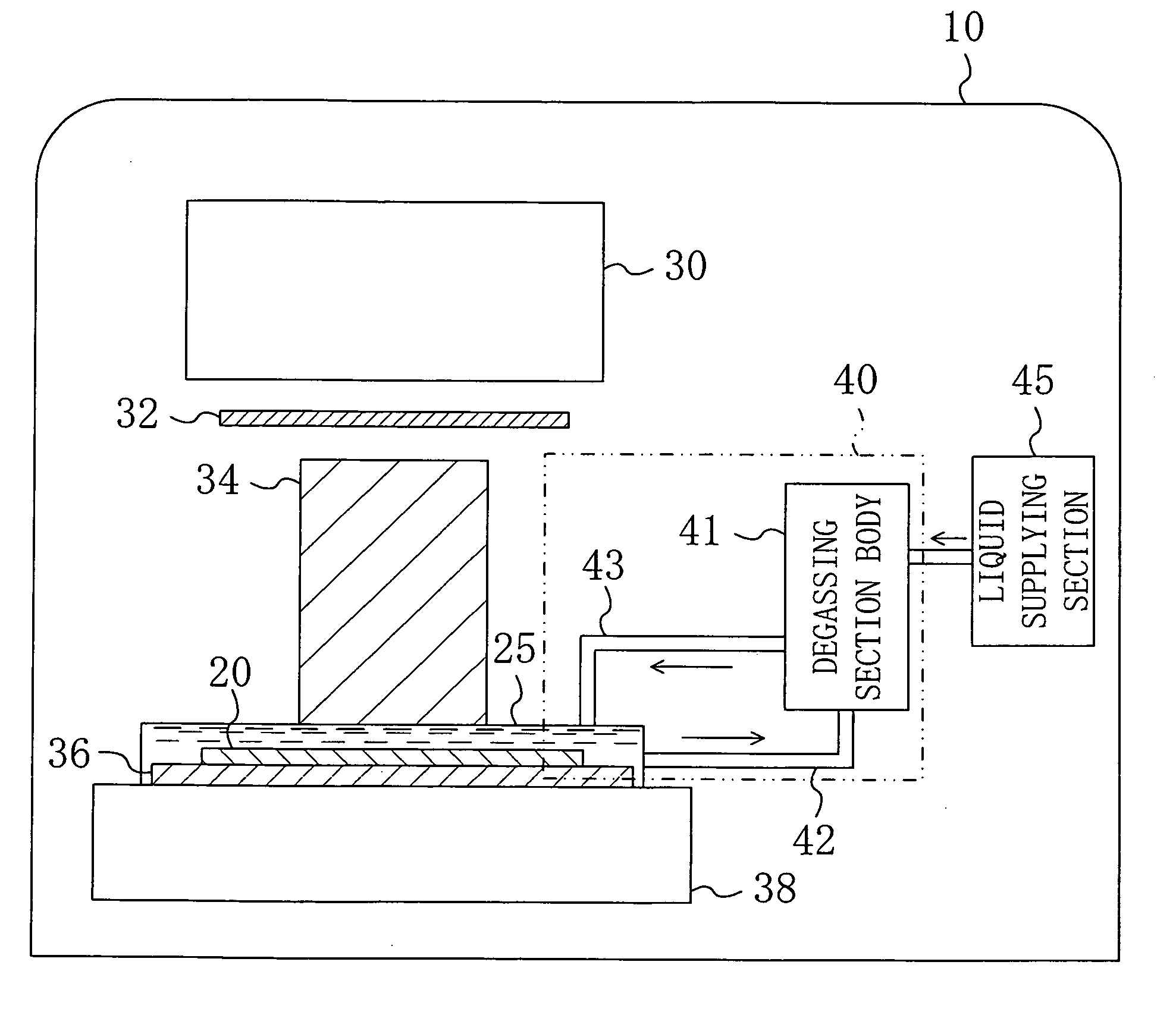
[0075]FIG. 3 schematically shows the cross-sectional structure of a principal part of a semiconductor manufacturing apparatus used for realizing a pattern formation method employing the immersion lithography according to the modification of Embodiment 1. In FIG. 3, like reference numerals are used to refer to like elements shown in FIG. 1 so as to omit the description.

[0076] As shown in FIG. 3, in the semiconductor manufacturing apparatus of this modification, a liquid 25 provided onto a wafer 20 is directly supplied from a liquid supplying section 45, and the liquid 25 having been provided onto the wafer 20 is degassed by a degassing section 40 during exposure. The liquid 25 supplied from the liquid supplying section 45 may or may not be previously degassed. Moreover, there is no need to always perform the degassing process but it may be appropriatel...

embodiment 2

[0079]FIG. 4 schematically shows the cross-sectional structure of a principal part of a semiconductor manufacturing apparatus used for realizing a pattern formation method employing the immersion lithography according to Embodiment 2 of the invention. In FIG. 4, like reference numerals are used to refer to like elements shown in FIG. 1 so as to omit the description.

[0080] As shown in FIG. 4, in the semiconductor manufacturing apparatus of Embodiment 2, a liquid used for increasing the value of the numerical aperture of exposing light is partially provided onto the principal surface of a wafer 20, namely, provided in the form of drops, instead of employing the pooling method of Embodiment 1 and the modification in which the whole wafer 20 is immersed in the liquid.

[0081] In the dropping method of this embodiment, the liquid 25 in the form of drops is allowed to flow during the movement of the movable stage 36 at a flow rate for preventing the air from being swallowed up into the li...

embodiment 3

[0095]FIG. 6 schematically shows the cross-sectional structure of a principal part of an exposure system, that is, a semiconductor manufacturing apparatus, used for realizing a pattern formation method employing the immersion lithography according to Embodiment 3 of the invention.

[0096] As shown in FIG. 6, the exposure system of Embodiment 3 includes an illumination optical system 130 provided within a chamber 110 and working as a light source for exposing a design pattern onto a resist film (not shown) applied on a wafer 120; and a liquid supplying section 140 for supplying, onto the resist film of the wafer 120, an immersion liquid 121A used for increasing the value of the numerical aperture of exposing light in the exposure.

[0097] Below the illumination optical system 130, a projection lens 131 for projecting, onto the resist film through the liquid 121A, the exposing light emitted from the illumination optical system 130 and entering through a mask (reticle) 122 having a desig...


PUM

PropertyMeasurementUnit
thicknessaaaaaaaaaa
temperatureaaaaaaaaaa
widthaaaaaaaaaa

Abstract

A semiconductor manufacturing apparatus includes a liquid supplying section for supplying a liquid onto a stage for holding a wafer on which a resist film is formed; an exposing section for irradiating the resist film with exposing light through a mask with the liquid provided on the resist film; and a removing part for removing, from the liquid, a gas included in the liquid. Thus, the liquid from which the gas has been removed is provided on the resist film, and therefore, foams included in the liquid or formed during the exposure can be removed. Accordingly, exposure abnormality such as diffraction abnormality can be prevented, resulting in forming a resist pattern in a good shape.

Description

CROSS-REFERENCE TO RELATED APLICATIONS [0001] This application claims priority under 35 U.S.C. § 119 on Patent Application Nos. 2003-383784 and 2004-146217 respectively filed in Japan on Nov. 13, 2003 and May 17, 2004, the entire contents of which are hereby incorporated by reference. BACKGROUND OF THE INVENTION [0002] The present invention relates to a semiconductor manufacturing apparatus used for manufacturing semiconductor integrated circuits by employing immersion lithography and a pattern formation method using the semiconductor manufacturing apparatus. [0003] In accordance with the increased degree of integration of semiconductor integrated circuits and downsizing of semiconductor devices, there are increasing demands for further rapid development of lithography technique. Currently, pattern formation is carried out through photolithography using exposing light of a mercury lamp, KrF excimer laser, ArF excimer laser or the like, and use of F2 laser lasing at a shorter wavelen...

Claims


Application Information

Patent Timeline
Patent Type & Authority Applications(United States)
IPC IPC(8): G03F7/20
CPCG03F7/70341
Inventor ENDO, MASAYUKISASAGO, MASARU
Owner RPX CORP
Why Eureka
Try Eureka