Transfer method, method of manufacturing thin film devices, method of maufacturing integrated circuits, circuit board and manufacturing method thereof, electro-optical apparatus and manufacturing method thereof, IC card, and electronic appliance

a technology of thin film devices and transfer methods, applied in the direction of non-linear optics, instruments, semiconductor/solid-state device details, etc., can solve the problems of inability to withstand such high temperatures, difficult to accurately align, and uncertainty in the placement of microstructures on the substra

Inactive Publication Date: 2005-05-19
SEIKO EPSON CORP
View PDF40 Cites 92 Cited by
  • Summary
  • Abstract
  • Description
  • Claims
  • Application Information

AI Technical Summary

Benefits of technology

[0017] According to the transfer method of the present invention, a plurality of transferred bodies such as devices or circuits that are to be disposed on a transfer destination substrate with spaces therebetween can be manufactured integrated together on a transfer origin substrate, and hence compared with the case that the transferred bodies are formed on the transfer destination substrate directly, the amount of materials used in the manufacture of the transferred bodies can be reduced, the area efficiency can be greatly improved, and a transfer destination substrate on which a large number of devices or circuits are disposed in scattered locations can be manufactured efficiently and cheaply.
[0065] The present invention also provides an IC card manufactured using a transfer method according to the present invention. According to the IC card of the present invention, a circuit board provided with devices or circuits that are IC card components is formed using a transfer method of the present invention, and hence the IC card has advantages similar to those of the electronic appliance of the present invention.

Problems solved by technology

However, with this microstructure technique, there is a drawback in that disposing the microstructures on the substrate with certainty and carrying out accurate alignment are difficult.
According to these transfer techniques, functional devices that require a high-temperature process during manufacture can be transferred onto desired substrates, including ones that cannot withstand such high temperatures.
However, with the conventional transfer techniques described above, there have been problems such as the following.
This is surprisingly troublesome, and hence there has been a problem that the manufacturing efficiency is prone to dropping.
Moreover, with the above transfer techniques, all of the thin film devices such as TFTs formed on the transfer origin substrate are transferred onto the transfer destination substrate, and hence the larger the area of the substrate, the better the properties, i.e. the higher the output power, the uniformity and so on, required of the laser light irradiated, and hence it becomes difficult to obtain a laser light source that meets the required performance, and moreover large, high-accuracy irradiation equipment becomes necessary for the laser light irradiation.
Furthermore, if laser light of high output power is irradiated, then there is a risk that the thin film devices may be heated to a temperature above the limit of heat resistance thereof, resulting in the functions of the thin film devices themselves being lost, and hence there has been a problem that the transfer process itself becomes difficult.

Method used


Image

  • Transfer method, method of manufacturing thin film devices, method of maufacturing integrated circuits, circuit board and manufacturing method thereof, electro-optical apparatus and manufacturing method thereof, IC card, and electronic appliance
  • Transfer method, method of manufacturing thin film devices, method of maufacturing integrated circuits, circuit board and manufacturing method thereof, electro-optical apparatus and manufacturing method thereof, IC card, and electronic appliance
  • Transfer method, method of manufacturing thin film devices, method of maufacturing integrated circuits, circuit board and manufacturing method thereof, electro-optical apparatus and manufacturing method thereof, IC card, and electronic appliance

Examples


first embodiment

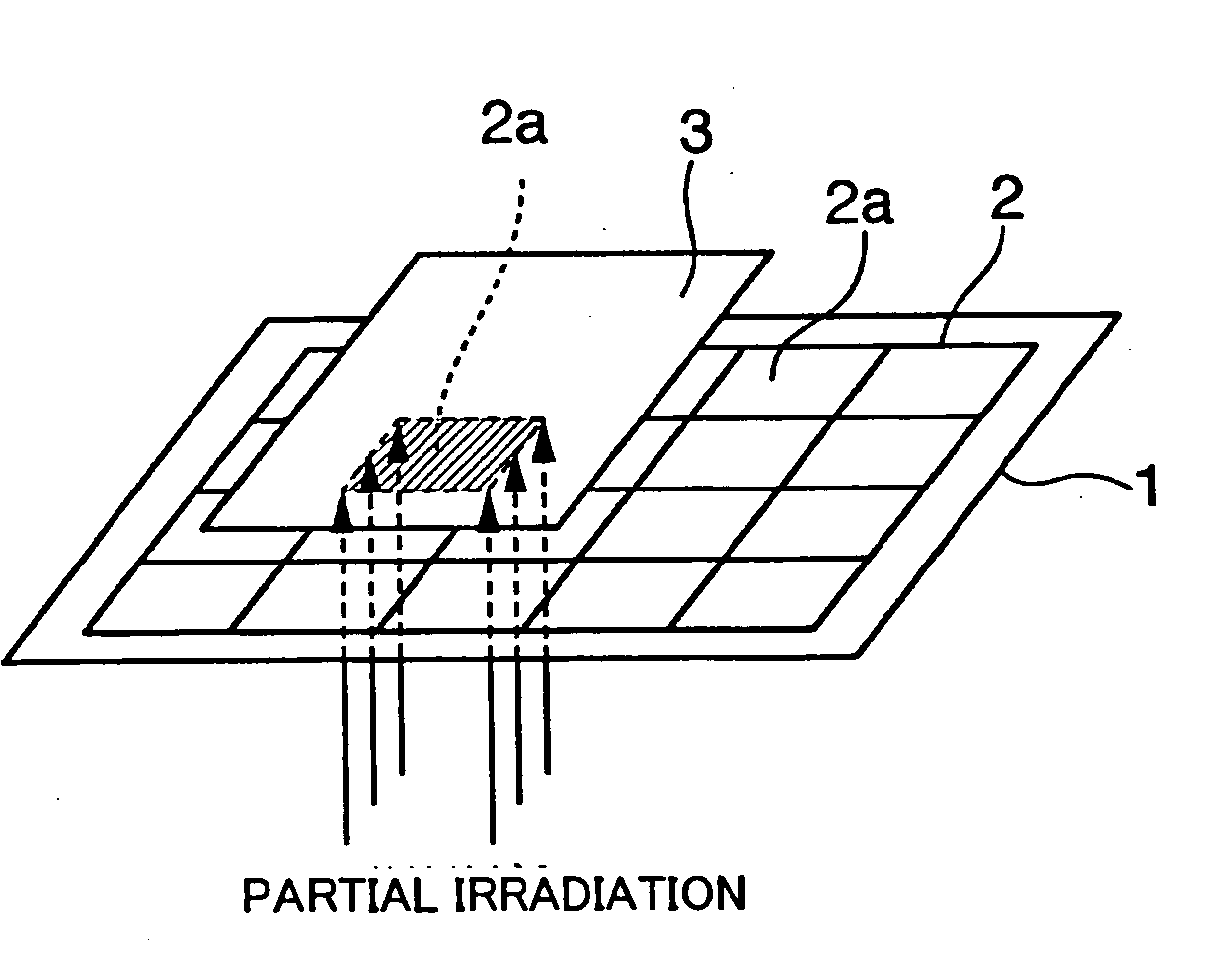
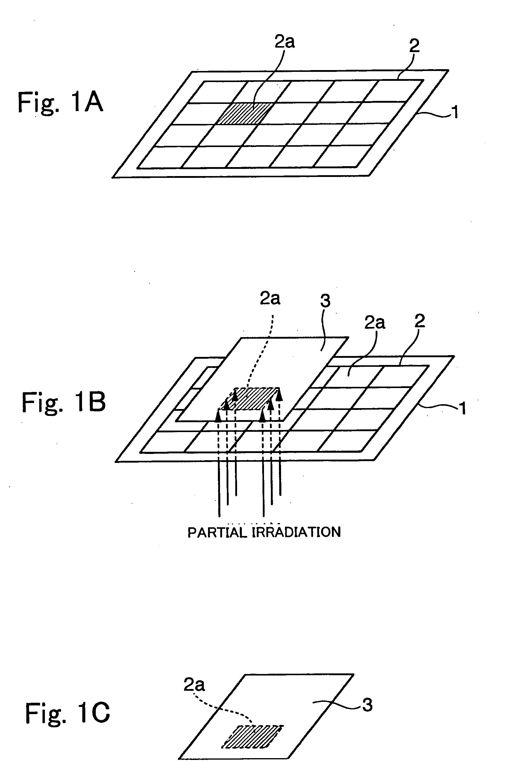
[0119]FIGS. 4A to 12B are drawings for explaining a first embodiment (transfer method) of the present invention. The first embodiment comes under the first invention, which relates to carrying out partial transfer once. The device transfer method is carried out through the following first to fifth steps.

[0120] In the first step, as shown in FIG. 4A, a peeling layer (light-absorbing layer) 11 is formed on a first substrate (transfer origin substrate) 10.

[0121] The first substrate 10 is preferably a light-transmitting substrate through which light can pass. As a result, light can be irradiated onto the peeling layer via the first substrate, and hence peeling can be made to occur swiftly and accurately through the irradiation of light onto the peeling layer. In this case, it is preferable for the transmissivity to light of the first substrate to be at least 10%, more preferably at least 50%. The higher the transmissivity, the lower the attenuation (loss) of light becomes, and hence t...

second embodiment

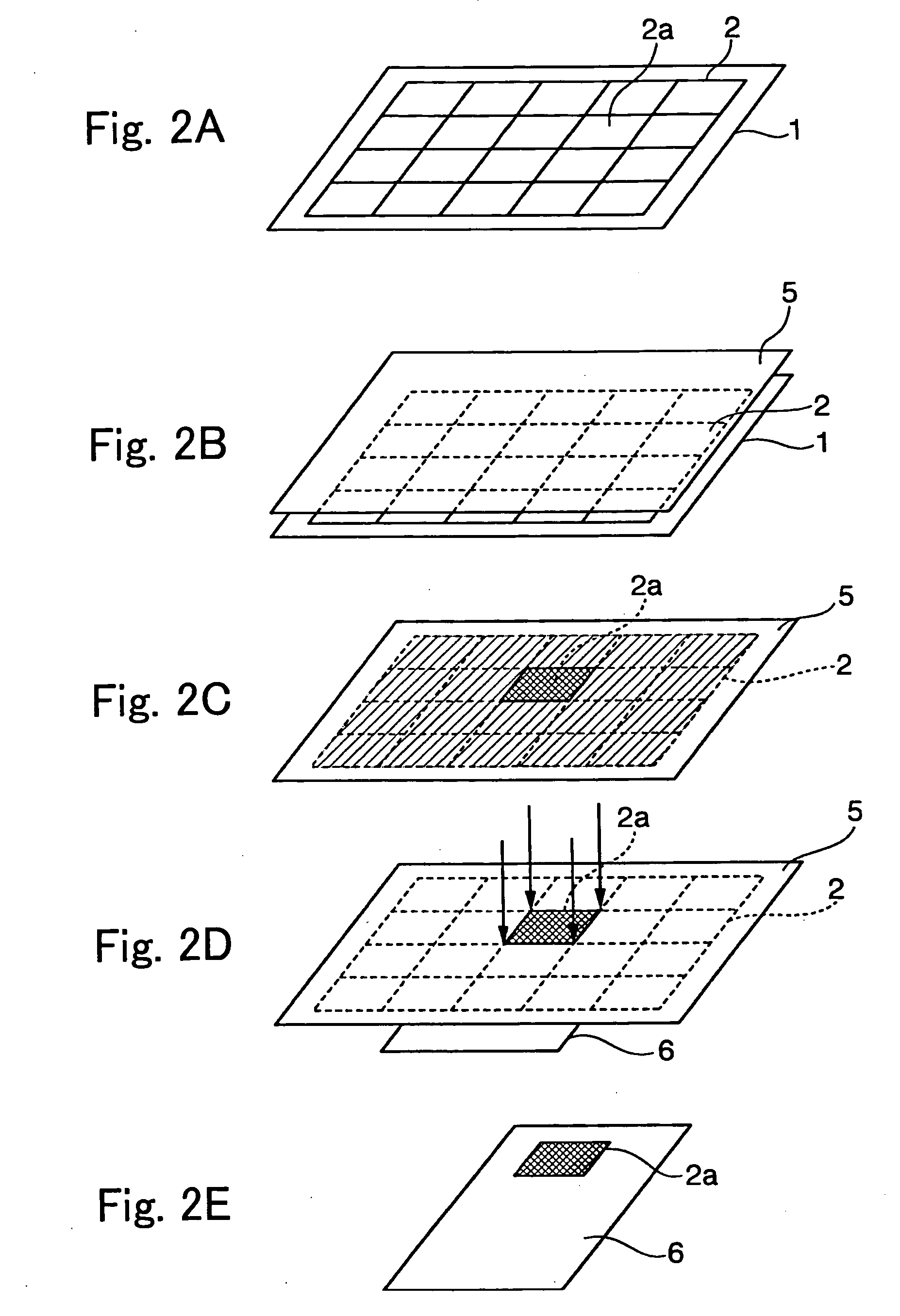
[0222]FIGS. 13A to 13D are drawings for explaining a second embodiment (transfer method) of the present invention. As with the first embodiment described above, the present second embodiment comes under the first invention, which relates to carrying out partial transfer once, but the present second embodiment differs from the first embodiment in particular in that, in the third step, the transferred bodies 12a to be transferred are joined to the final substrate 14 through a combination of a UV-curing resin and partial irradiation with UV light.

[0223] The first step and the second step can be carried out as in the first embodiment described above with regard to the methods of operation, components and materials used, formation conditions and so on, and hence the description of these steps will be omitted here.

[0224] In this second embodiment, a first substrate 10 having a large number of transferred bodies 12a formed thereon, and a final substrate 14 having an adhesive layer 52 com...

third embodiment

[0233]FIGS. 14A and 14B are drawings for explaining a third embodiment (transfer method) of the present invention. As with the first embodiment described above, the present third embodiment comes under the first invention, which relates to carrying out partial transfer once, but the present third embodiment differs from the first embodiment in particular in that, in the third step, the transferred bodies 12a to be transferred are joined to the final substrate 14 through a combination of an adhesive sheet 56 comprising a heat-fusing adhesive disposed between the final substrate 14 and the transferred bodies 12a and partial irradiation with laser light L1.

[0234] The first step and the second step can be carried out as in the first embodiment described above with regard to the methods of operation, components and materials used, formation conditions and so on, and hence the description of these steps will be omitted here.

[0235] In this third embodiment, adhesive (heat-fusing) sheets ...


PUM


Abstract

A transfer method comprising a step of forming a plurality of transferred bodies on a transfer origin substrate, and a step of applying energy to partial regions corresponding to the transferred bodies to be transferred, and transferring these transferred bodies corresponding to the partial regions onto a transfer destination substrate. A plurality of transferred bodies such as devices or circuits that are to be disposed on a transfer destination substrate with spaces therebetween can be manufactured integrated together on a transfer origin substrate, and hence compared with the case that the transferred bodies are formed on the transfer destination substrate directly, the amount of materials used in the manufacture of the transferred bodies can be reduced, the area efficiency can be greatly improved, and a transfer destination substrate on which a large number of devices or circuits are disposed in scattered locations can be manufactured efficiently and cheaply.

Description

[0001] This is a Division of application Ser. No. 10 / 201,268 filed Jul. 24, 2002. The entire disclosure of the prior application is hereby incorporated by reference herein.BACKGROUND OF THE INVENTION [0002] 1. Field of the Invention [0003] The present invention relates to a transfer method for devices or circuits, and a circuit board, an electro-optical apparatus, an IC card and an electronic appliance manufactured using the transfer method. [0004] 2. Description of the Related Art [0005] Recently, with regard to the manufacture of electro-optical apparatuses such as liquid crystal electro-optical apparatuses having thin film devices such as thin film transistors (TFTs) or thin film diodes (TFDs), there has been research into various art for reducing the amount of thin film device-constituting material discarded through etching and thus greatly reducing the manufacturing cost of the electro-optical apparatuses. [0006] Conventionally, a method developed by Alien Technology called the...

Claims


Application Information

Patent Timeline
Patent Type & Authority Applications(United States)
IPC IPC(8): H01L21/336H01L21/77H01L21/8242H01L21/8244H01L21/8246H01L21/8247H01L21/84H01L27/118H01L27/13H01L27/32H01L51/56H05K3/04
CPCB82Y10/00H01L21/6836G02F2001/13613H01L27/10844H01L27/11H01L27/11213H01L27/11502H01L27/11517H01L27/11585H01L27/1159H01L27/118H01L27/1214H01L27/1266H01L27/13H01L27/3244H01L29/66757H01L29/66772H01L51/56H01L2221/68318H01L2221/68322H01L2221/68359H01L2221/68363H01L2221/68368H01L2225/06562H05K3/046H01L21/6835H01L2221/6835H01L2221/68381B82Y30/00H01L2224/95G02F1/13613H10B12/01H10B10/00H10B20/27H10B53/00H10B41/00H10B51/00H10B51/30H10K59/12H10K71/00
Inventor SHIMODA, TATSUYAUTSUNOMIYA, SUMIO
Owner SEIKO EPSON CORP
Why Eureka
Try Eureka