High light efficiency of GaN-series of light emitting diode and its manufacturing method thereof

Inactive Publication Date: 2005-05-26
SUPERNOVA OPTOELECTRONICS
View PDF6 Cites 14 Cited by
  • Summary
  • Abstract
  • Description
  • Claims
  • Application Information

AI Technical Summary

Benefits of technology

[0011] The primary purpose of the present invention is to provide a high light efficiency of GaN-series of light emitting diode and its manufacturing method, wherein controlling the strain of the follow mentioned two layers while epitaxially growing a p-type cladding layer and a p-type transition layer is formed on the said cladding layer, then forms a p-type ohmic contact layer on the said p-type transition layer, which makes the surface of p-type semiconductor layer having textured structure. The optical waveguide effect can be interrupted and increase external quantum efficiency through the said textured structure.
[0012] The secondary purpose of the present invention is to provide a high light efficiency of GaN-series of light emitting diode and its manufacturing method, wherein the generation method of the said p-type semiconductor layer enables to reduce the generation possibility of h

Problems solved by technology

Hence, the extracting efficinecy of said light emitting diode is limited by the absorption of the semi-transparent metal conductive layer and reabsorption of internal epitaxial structure.
However, because the method one requires utilizing a method of mechanical polishing or chemical etching to produce said rough texturing so it easily causes the non-uniformity of surface roughness on the sapphire substrate and then influence the conditions of next epitaxial structure and also not easily to control the manufacturing yield.
Besides, the method two increases the complexity of fabrication and manufacturing cost because of making tunnel channels and embedded mater

Method used


Image

  • High light efficiency of GaN-series of light emitting diode and its manufacturing method thereof
  • High light efficiency of GaN-series of light emitting diode and its manufacturing method thereof
  • High light efficiency of GaN-series of light emitting diode and its manufacturing method thereof

Examples


Embodiment Construction

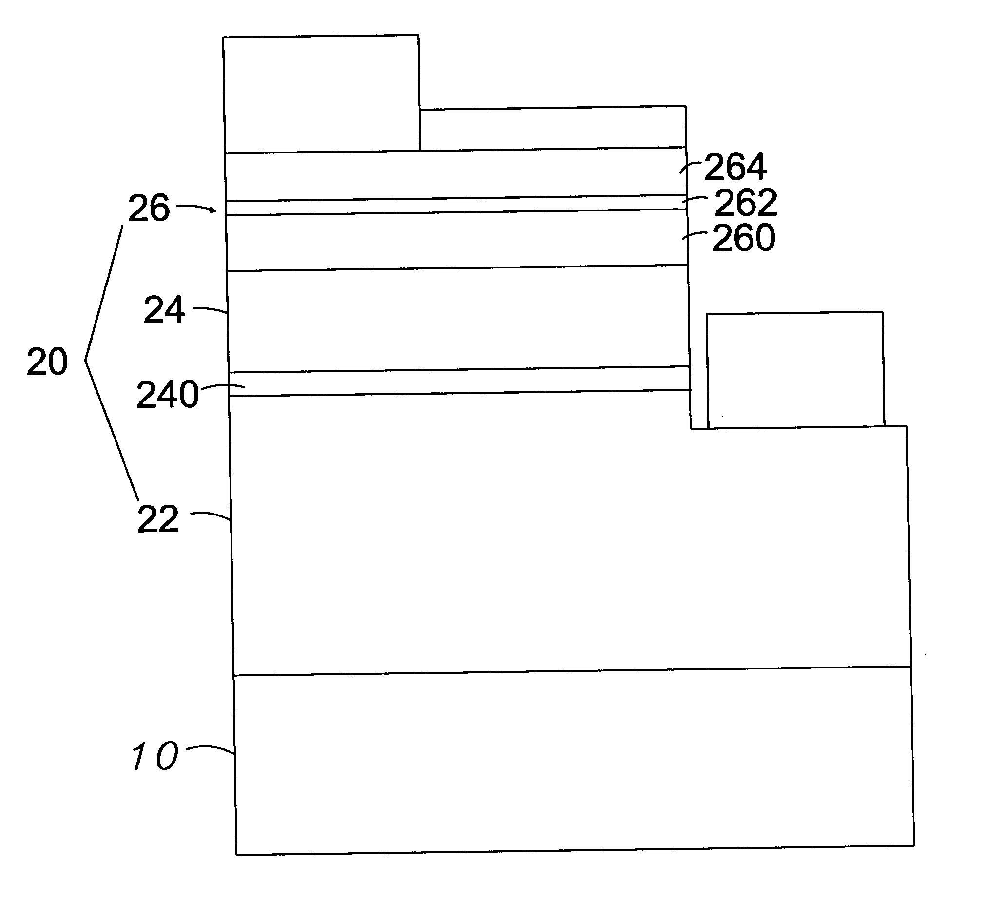
[0018] In order to clearly express and explore the feature characteristics and efficiency of the present invention for the committee of patent, the preferred embodiment and detailed description is as below.

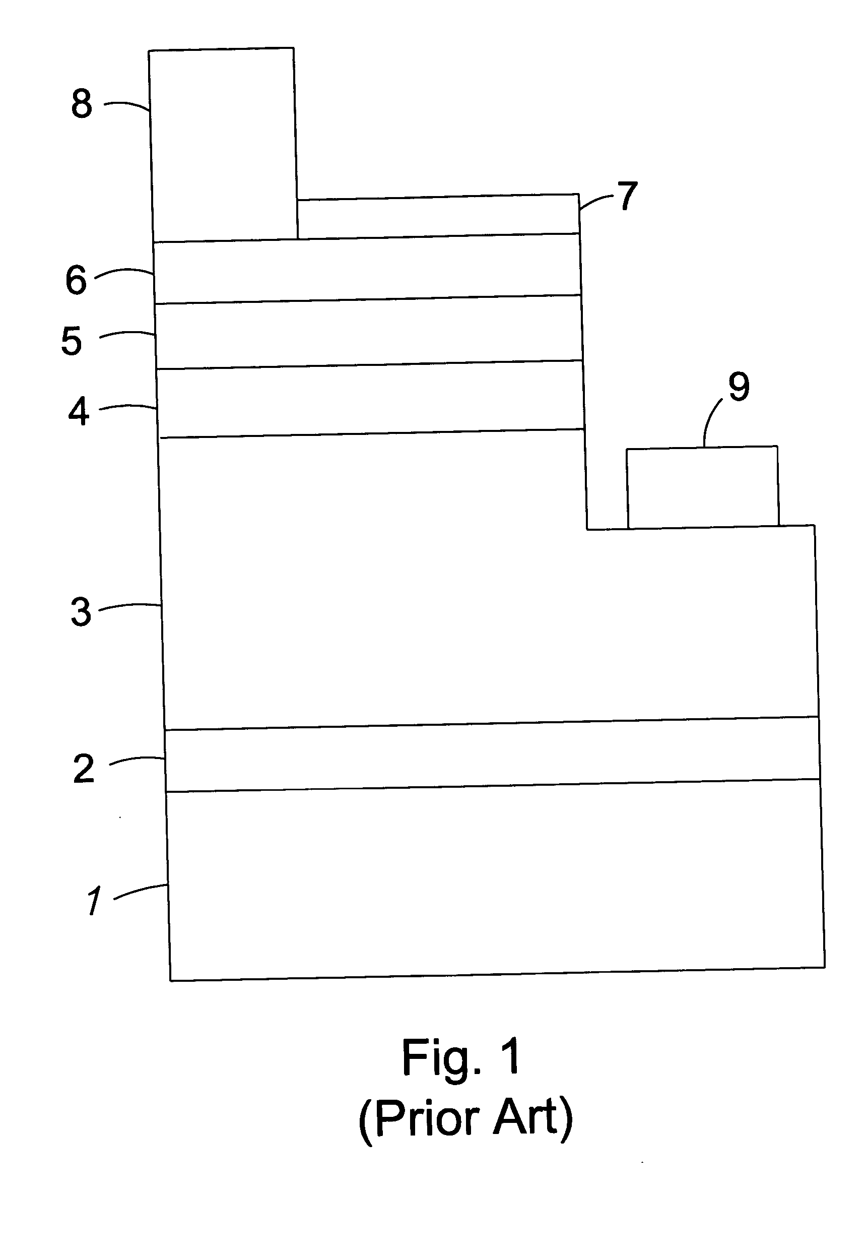
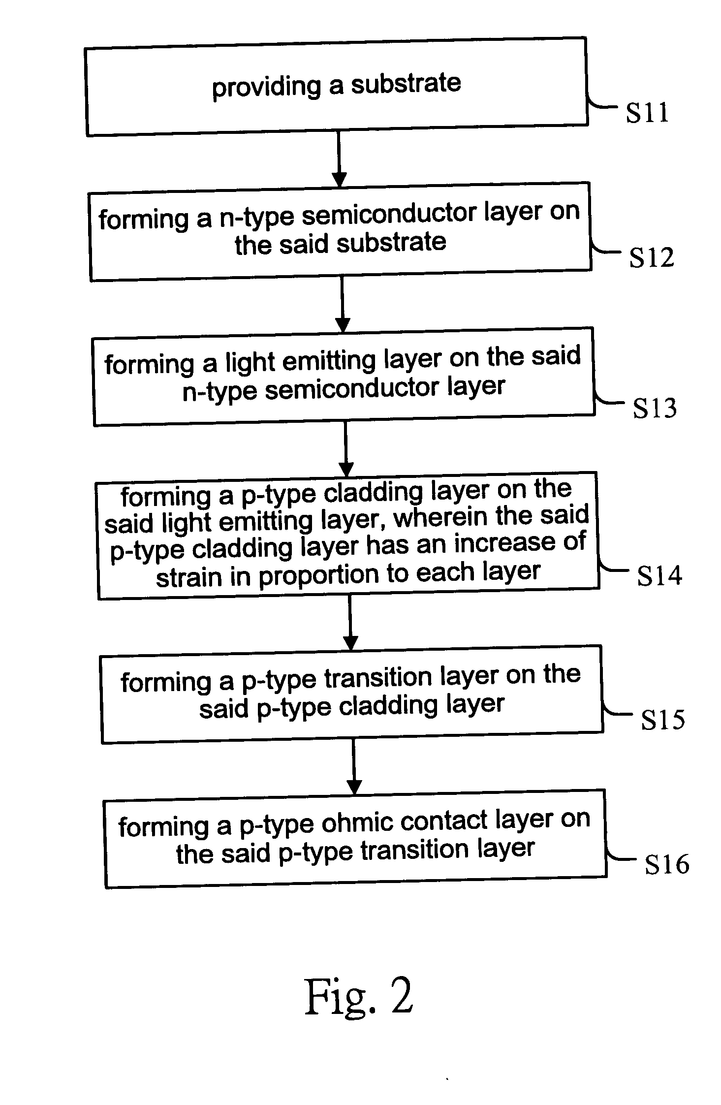
[0019] The present invention is a method and a structure of interrupting optical waveguide effect and aims to solve the prior arts which all apply for post process such as mechanical polishing, or chemical etching or the disclosed method by the MOCVD epitaxy skill to generate the textured surface that easily makes hexagonal shaped pits and then causes in the operation life short and the production yield is not controllable, Hence, the process and structure of the present invention are novel arts which do not require the post machining process and not cause in hexagonal shaped pits Firstly, refer to FIG. 2 which illustrates the manufacturing flow chart of one of the preferred embodiment of light emitting diode of the present invention, which comprises the steps of [0020] Step 11: ...


PUM


Abstract

A high light efficiency of GaN-series of light emitting diode and its manufacturing method thereof disclose a process and structure of a p-type semiconductor layer of surface texture structure generation. The optical waveguide effect can be interrupted and the possibility of hexagonal shaped pits defect generated can be reduced through said texture structure. The method explores that controlling the tension and compression of strain while a p-type cladding layer and a p-type transition layer are generated, and then a p-type ohmic contact is formed on said p-type transition layer. Through the control and its structure of said epitaxial growth process, the surface of said p-type semiconductor layer is with texture structure to increase external quantum efficiency and its operation life.

Description

BACKGROUND OF THE INVENTION [0001] 1. Field of the Invention [0002] The present invention relates to a high light efficiency of GaN-series of light emitting diode and its manufacturing method thereof, especially for a GaN-series light emitting diode and its manufacturing method thereof, which using controlling the strain of epitaxy layer during the process of epitaxial growth to form a p-type semiconductor layer with surface textured structure to interrupt the optical waveguide effect. [0003] 2. Description of the Related Art [0004] Using sapphire substrate grown GaN-series light emitting diode, according to prior art, shows as FIG. 1 which is so-called conventional structure, wherein consisting of a GaN buffer layer 2, a n-type GaN ohmic contact 3, a InGaN light emitting layer 4, a p-type AlGaN cladding layer 5 and a p-type GaN ohmic contact layer 6 of epitaxially grown sequentially on the sapphire substrate 1, wherein making a semi-transparent metal conductive layer 7 on the p-typ...

Claims


Application Information

Patent Timeline
IPC IPC(8): H01L33/06H01L33/10H01L33/22H01L33/28H01L33/32H01L33/34
CPCH01L33/32H01L33/22E04H9/14
Inventor LAI, MU-JENHON, SCHANG-JING
Owner SUPERNOVA OPTOELECTRONICS
Why Eureka
Try Eureka