Solid state imaging device and producing method thereof

a technology of solid-state imaging and production method, which is applied in the direction of semiconductor devices, radiation controlled devices, semiconductor/solid-state device details, etc., can solve the problems of increasing the number of expensive operations or production lines, and reducing the number of operations. , the effect of deteriorating image quality

Inactive Publication Date: 2005-05-26
FUJIFILM HLDG CORP +1
View PDF2 Cites 22 Cited by
  • Summary
  • Abstract
  • Description
  • Claims
  • Application Information

AI Technical Summary

Benefits of technology

[0020] An object of the present invention is to provide a solid state imaging device, in which interconnections can be exposed on a bottom of the semiconductor substrate in a low cost.
[0028] According to the solid state imaging device and a producing method thereof, since the bumps are used instead of through-hole interconnections, the deterioration of the image quality caused by the voids in the through-hole interconnections does not occur. Further, the operations of the high cost, for example the insulation layer in the through-hole, the remove of the insulation layer on the contact terminal, vacuum screen print and the like can be omitted, the number of the operations can be reduced and the solid state imaging device can be produced in low cost.
[0029] Further, since the grinding of the wafer is made before forming the through-holes, the thickness of the solid state imaging device can be decreased. Further, since the etching for forming the through-holes can be completed in a sort time, the productivity becomes higher, the cost becomes lower, and the side etch is prevented. If the grinding of only the wafer is made, the strength extremely decreases, and therefore the handling and the like are difficult. However, since the grinding of the wafer joined to the translucent substrate, the strength can be kept enough for the handling.
[0030] Further, since a DSP chip and the like can be assembled with face down, the apparatus in which the solid state imaging device is used can become smaller. Further, since the contact terminals are sealed by the translucent member, the width of sealing becomes larger. Therefore the sealing effective increases.
[0031] Since there is a space between the image sensor and the translucent member, the solid state imaging device is provided with micro lenses above respective pixels having photoelectric function, and the effectives of the micro lenses don't become lower. Further, the said translucent member is one of a low-α-ray glass, IR-cut filter and a low path filter, an space and works for attachment can be made smaller than when they are separately attached. Further, since a spacer is disposed between the translucent member and the semiconductor substrate, the sealing can be made by forming a gap above the image sensor, instead of processing, such as forming the recess of the translucent member. Further, since a material of the spacer is silicon and the like whose coefficient of thermal expansion is near that of the wafer, the generation of the image sensor does not cause the stress between the spacer and the semiconductor substrate and the spacer does not broken in the effect of the stress.
[0032] Further, since the through-holes are formed after sealing the image sensor, the productivity does not become lower. Furthermore, the sealing is complete in the size of the wafer, a movement accuracy of the semiconductore substrate and the positioning accuracy in XYZ directions can be extremely improved. In this case, even when the solid state imaging device is loaded on a camera module and the like on the basis of the outer shape, it is not necessary to adjust the position of image pick-up.

Problems solved by technology

However, in this case, the assembling size actually becomes large.
Accordingly, dusts and cruds are easily adhered onto the imaging elements, and the production yield becomes lower.
Thus, the number of the expensive operations and the total processes or operations in the production line becomes increased.
Accordingly, the solid state imaging device becomes expensive.
Further, the solid state imaging device of the CSP structure or the WLCSP structure becomes small, and therefore the pitch of interconnection is short.
In this case, the through-hole interconnections easily have voids caused by insufficient supply of the conductive paste, and the voids change the resistance.
Especially in the solid state imaging device, the change of the resistance of the through-hole interconnection disrupts the output waveform, and the image quality became worse.

Method used


Image

  • Solid state imaging device and producing method thereof
  • Solid state imaging device and producing method thereof
  • Solid state imaging device and producing method thereof

Examples


Embodiment Construction

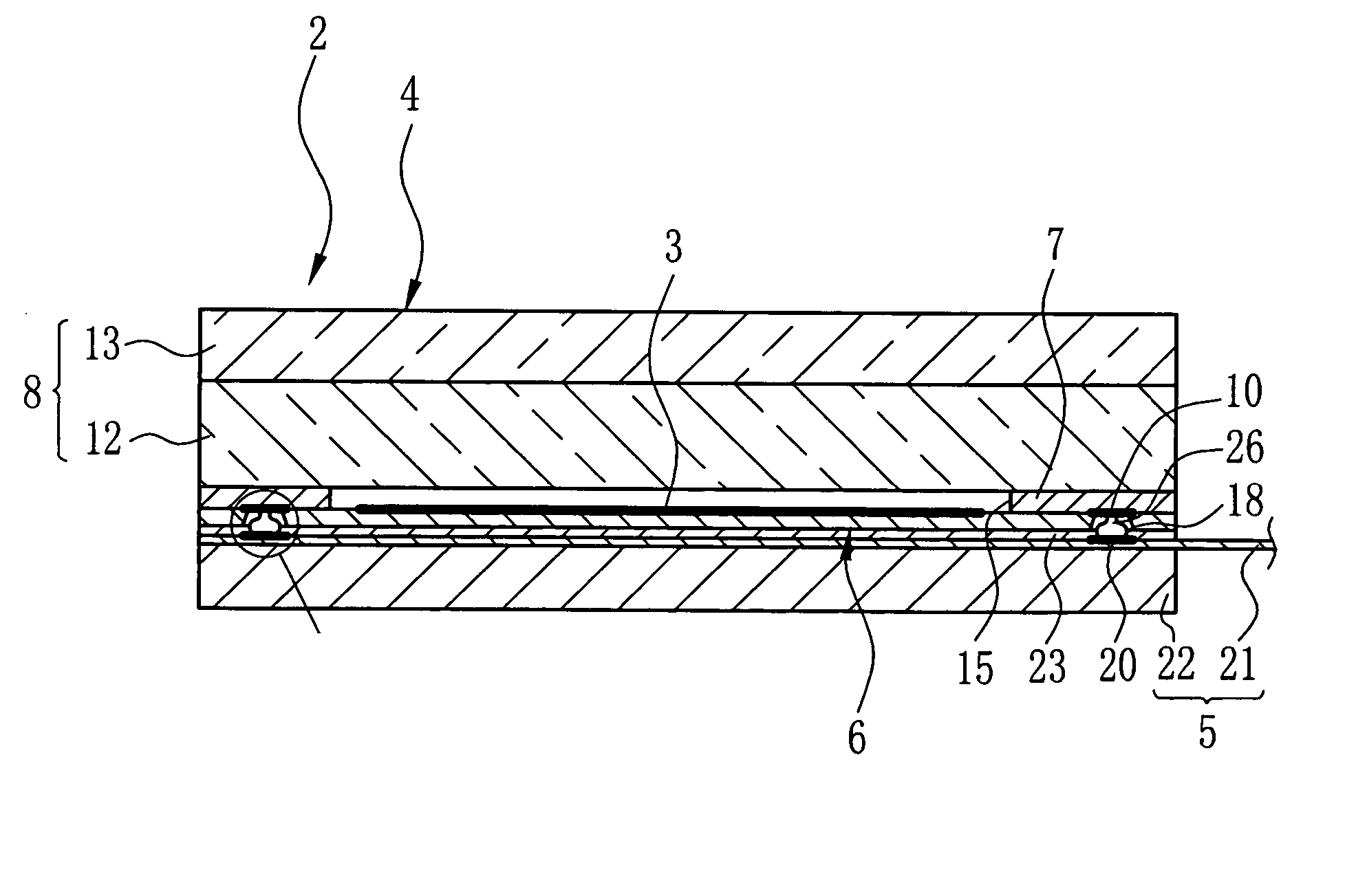
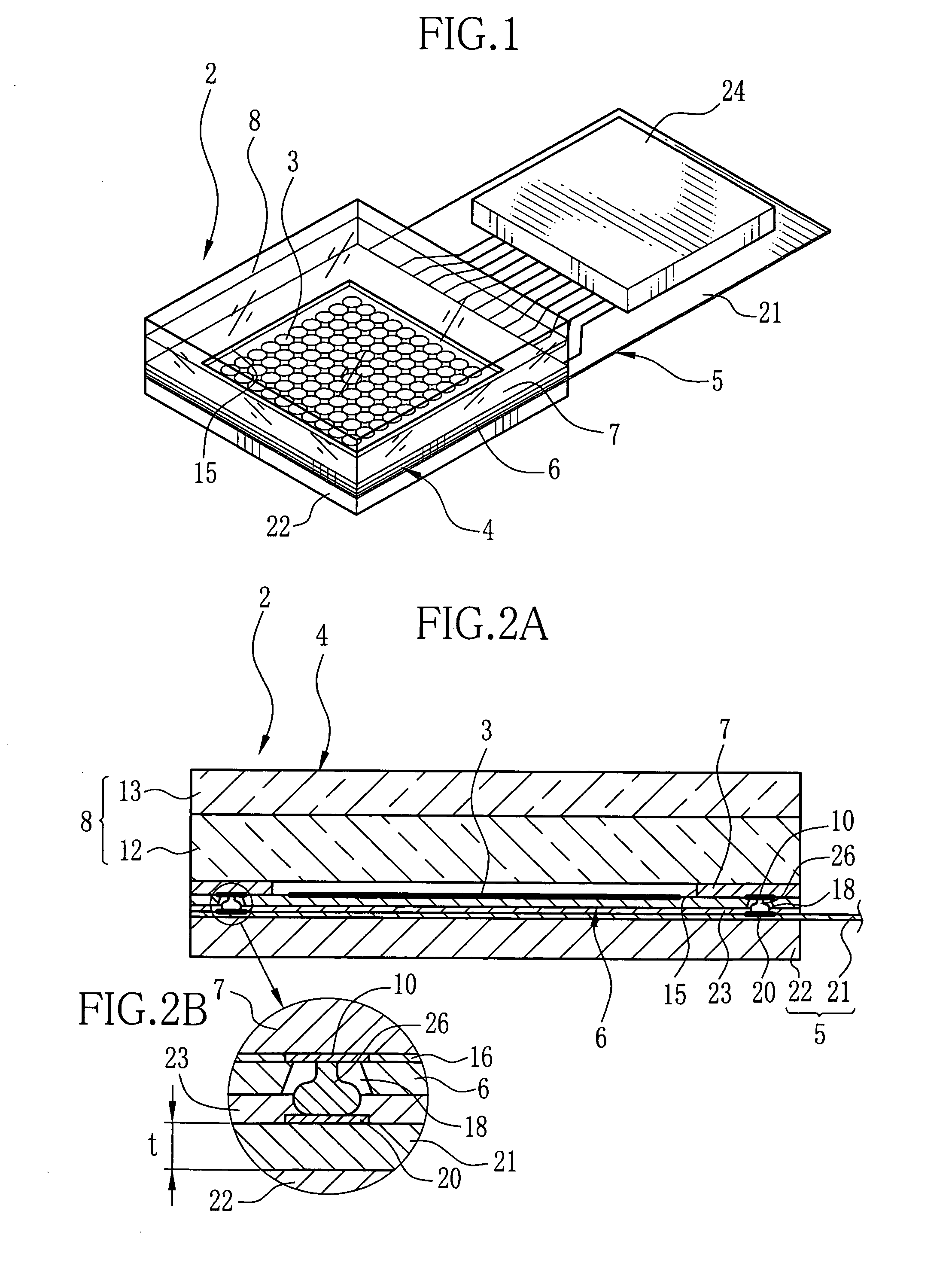
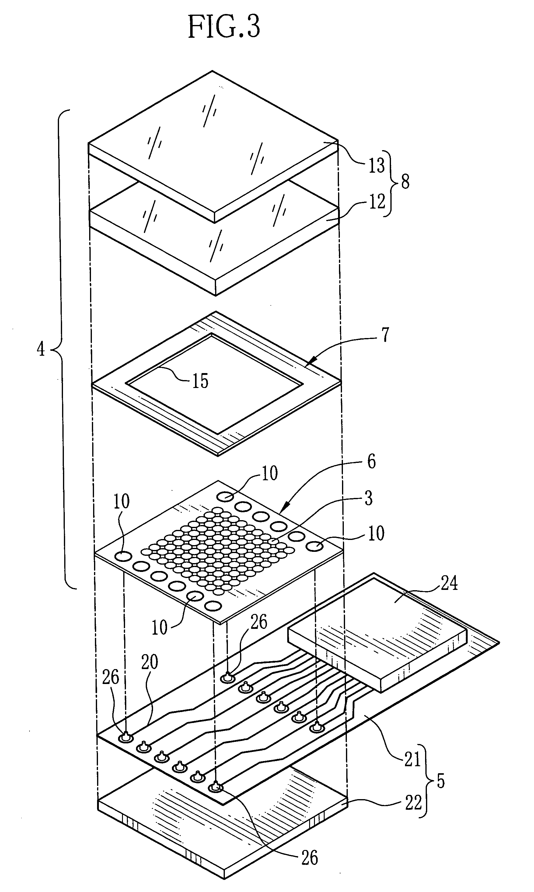
[0051] In FIGS. 1-3, the solid state imaging device 2 has a WLCSP structure and is constructed of a rectangular imaging chip 4 which is provided with image sensors 3 and an assembly substrate 5 on which the imaging chip 4 is assembled. The imaging chip 4 includes a semiconductor substrate 6 on whose upper face the image sensors 3 are formed, a frame-like spacer 7 which is attached onto the semiconductor substrate 6 so as to surround the image sensors 3, and a cover glass 8 as a translucent member or a translucent substrate. The cover glass 8 is disposed above the spacer 7 so as to tightly close the image sensors 3.

[0052] The semiconductor substrate 6 is obtained by dividing a silicon wafer so as to have a rectangular shape, and has the image sensors 3 in a central area of an upper face and plural contact terminals 10 arranged on the confronting two edges. The thickness t of the semiconductor substrate 6 is decreased, for example in the range of 30 μm to 100 μm, and preferably to ab...


PUM


Abstract

A semiconductor substrate of a solid state imaging device is connected to a cover glass, and then a backgrind is performed so as to make the thickness smaller. On a first face of the semiconductor substrate is formed plural units which is constructed of image sensors and plural contact terminals. At positions of the contact terminals, plural through-holes are formed on the bottom side of the semiconductor substrate, and the contact terminals appear on a second surface of the semiconductor substrate. On an interconnection circuit pattern of the assembly substrate are formed stud bumps. When the semiconductor substrate is assembled onto the assembly substrate, the stud bumps enter into the through-holes to contact to the contact terminals. Thus the interconnection circuit pattern is electrically connected to the image sensors.

Description

BACKGROUND OF THE INVENTION [0001] 1. Field of the Invention [0002] The present invention relates to a solid state imaging device with a wafer-level chip size package, and more particularly to a solid state imaging device in which a wiring is extended to an opposite surface to a photoelectric conversion surface, and a producing method of the solid state imaging device. [0003] 2. Description Related to the Prior Art [0004] A digital video camera and a video camera with use of solid state imaging device (such as CCDs, CMOS type and the like) is in wide spread use. Further, an electronic apparatus (a personal computer, a mobile phone, an electronic notepads or the like) includes a solid state imaging device and a memory to have an image-taking function. Since having a large influence on an outer size of a digital camera or an electronic apparatus with the image-taking function, the solid state imaging device is required to be small. [0005] In order to make the solid state imaging devic...

Claims


Application Information

Patent Timeline
Patent Type & Authority Applications(United States)
IPC IPC(8): H01L27/14H01L23/00H01L23/02H01L27/146
CPCH01L27/14618H01L27/14632H01L27/14634H01L2224/73204H01L27/14683H01L27/14687H01L27/1469H01L27/14636H01L23/00H01L27/14
Inventor YAMAMOTO, KIYOFUMINISHIDA, KAZUHIRO
Owner FUJIFILM HLDG CORP
Why Eureka
Try Eureka