Method for forming a multi-layer seed layer for improved Cu ECP

Inactive Publication Date: 2005-05-26
TAIWAN SEMICON MFG CO LTD
View PDF16 Cites 75 Cited by
  • Summary
  • Abstract
  • Description
  • Claims
  • Application Information

AI Technical Summary

Problems solved by technology

In addition, the aspect ratios (height/width) of interconnect openings becomes increasingly large, making continuous coverage of physical vapor deposition (PVD) process more problematical.
For example, the presence of a relatively rough surface due to the penetration of pore openings at the surface of an opening etched into a low-K IMD layer produces surface micro-adversely affecting coverage of overlying deposited layers, for example diffusion barrier layers and seed layers.
Further, the deposition of seed layers, typically formed by PVD processes, may be non-continuously f

Method used


Image

  • Method for forming a multi-layer seed layer for improved Cu ECP
  • Method for forming a multi-layer seed layer for improved Cu ECP
  • Method for forming a multi-layer seed layer for improved Cu ECP

Examples


Embodiment Construction

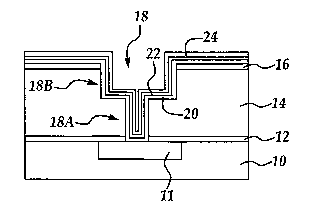
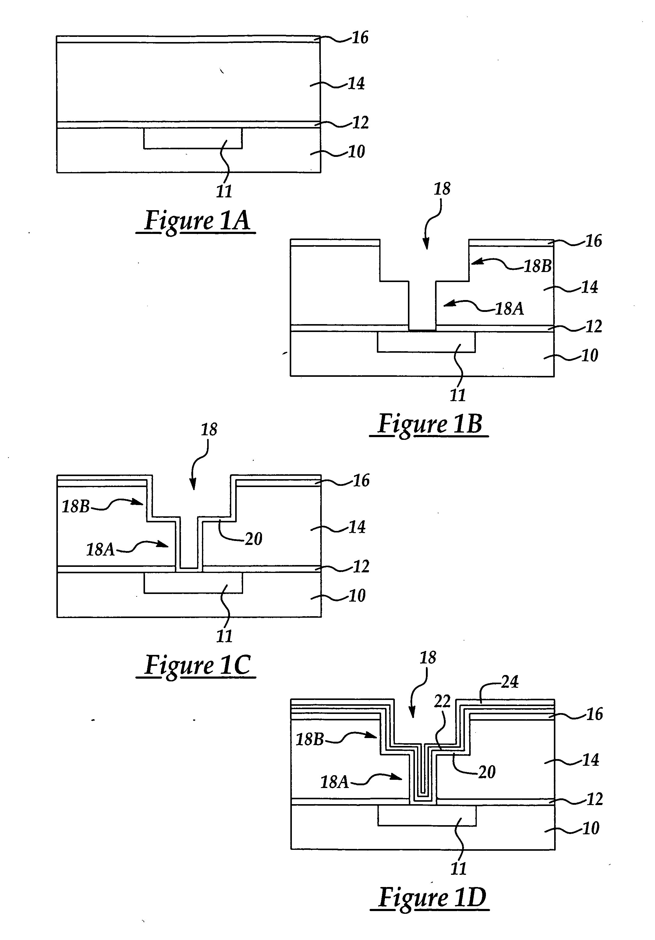
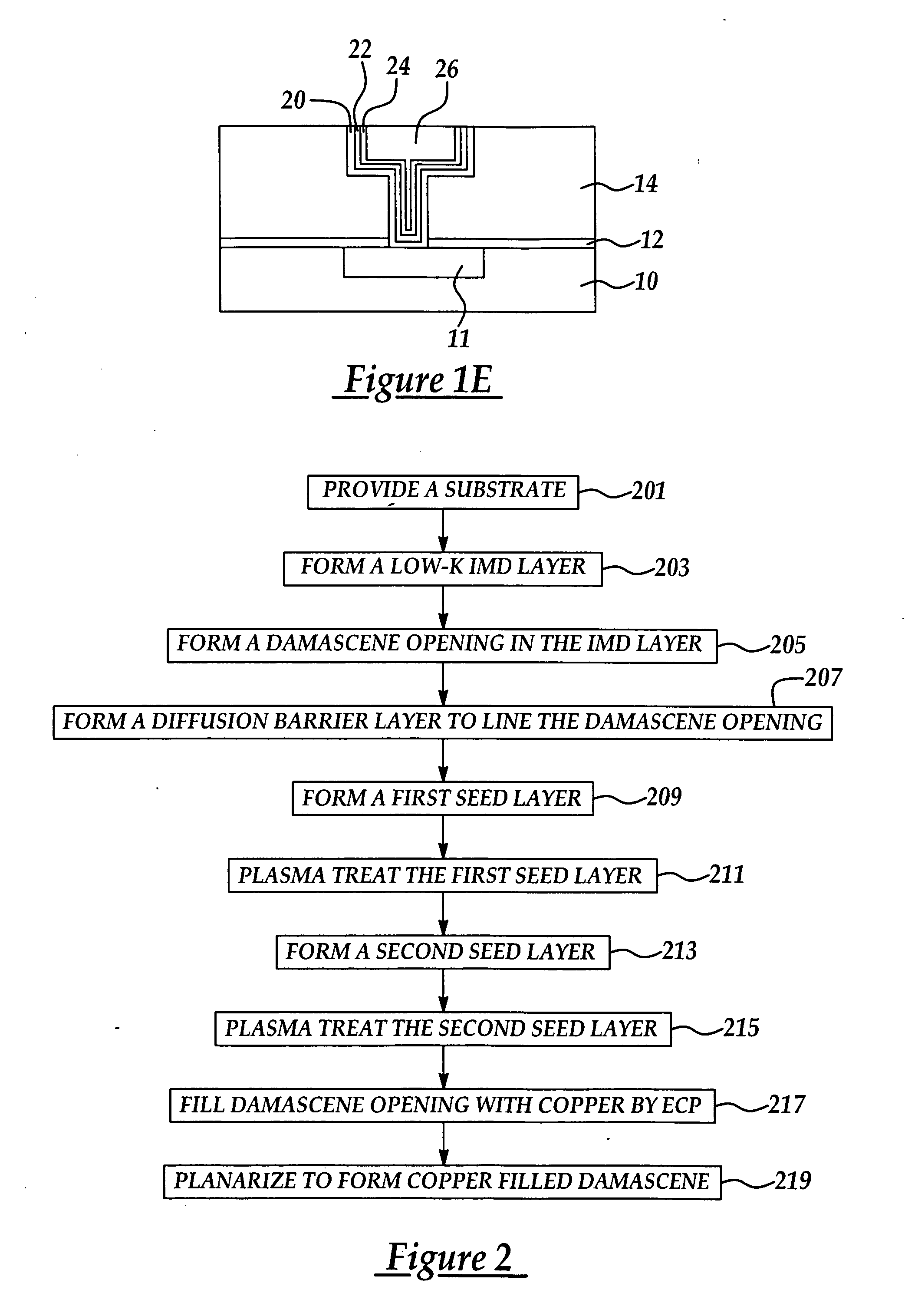
[0014] Although the present invention is explained by reference to an exemplary dual damascene formation process, it will be that the method of the present invention applies generally to the formation of damascenes including single vias and trench lines extending through single or multiple IMD layers. While the method is particularly advantageous for forming copper damascenes in porous low-K dielectrics, it will be appreciated that the method may be applied to the formation of other metal damascenes and other dielectric insulating layers, particularly where damascene opening aspect ratios are greater than about 4, where the method of the present invention will advantageously improve step coverage of seed layers to improve a copper ECP process.

[0015] By the term damascene is meant any damascene interconnect structure both e.g., both single and dual damascenes, including vias, contact openings, and trench lines. Further, the term ‘copper’ will be understood to include copper and allo...


PUM


Abstract

A copper filled damascene structure and method for forming the same the method including providing a substrate comprising a semiconductor substrate; forming an insulator layer on the substrate; forming a damascene opening through a thickness portion of the insulator layer; forming a diffusion barrier layer to line the damascene opening; forming a first seed layer overlying the diffusion barrier; plasma treating the first seed layer in-situ with a first treatment plasma comprising plasma source gases selected from the group consisting of argon, nitrogen, hydrogen, and NH3; forming a second seed layer overlying the first seed layer; forming a copper layer overlying the second seed layer according to an electro-chemical plating (ECP) process to fill the damascene opening; and, planarizing the copper layer to form a metal interconnect structure.

Description

FIELD OF THE INVENTION [0001] This invention generally relates to semiconductor device manufacturing methods and more particularly to a method for forming copper damascenes within low-K dielectric insulating layers including forming a multi-layer seed layer to improve a copper ECP process to fill a copper damascene. BACKGROUND OF THE INVENTION [0002] In forming damascene structures in integrated circuit manufacturing processes, the surface condition of the damascene opening is critical for achieving acceptable adhesion and coverage of overlying layers. The damascene opening, for example a dual damascene opening is formed in an inter-metal dielectric (IMD) insulating layer by a series of photolithographic patterning and etching processes, followed by formation of a barrier layer and overlying metal, e.g., copper, seed layer to promote a copper electro-chemical plating (ECP) deposition process. [0003] Increasingly, low-K IMD layers are required to reduce signal delay and power loss ef...

Claims


Application Information

Patent Timeline
IPC IPC(8): H01L23/532
CPCH01L21/76807H01L21/76846H01L23/53295H01L21/76873H01L23/53238H01L21/76862H01L2221/1089H01L2924/0002H01L2924/00
Inventor WU, PING-KUNTSENG, HORNG-HUEILO, CHINE-GIEWANG, CHAO-HSIUNGSHUE, SHAU-LIN
Owner TAIWAN SEMICON MFG CO LTD
Why Eureka
Try Eureka