Method and apparatus for forming thin films, method for manufacturing solar cell, and solar cell

Inactive Publication Date: 2005-06-02
IHI CORP
View PDF1 Cites 43 Cited by
  • Summary
  • Abstract
  • Description
  • Claims
  • Application Information

AI Technical Summary

Benefits of technology

[0031] As described above, according to the apparatus for forming thin films, which is the first aspect of the present invention, impurities in the chamber are removed, with the effect that autodoping can be suppressed, and favorable solar cell properties can be obtained. Also, because a plura

Problems solved by technology

However, the properties of a solar cell manufactured by a single chamber deposition process are inferior to one manufactured by a system which deposits different kinds of thin films using separate chambers (a separate deposition system).
For example, in the above process for manufacturing a solar cell, doping (auto-doping) the i-type semiconductor layer and the n-type semiconductor layer has been a pro

Method used


Image

  • Method and apparatus for forming thin films, method for manufacturing solar cell, and solar cell
  • Method and apparatus for forming thin films, method for manufacturing solar cell, and solar cell
  • Method and apparatus for forming thin films, method for manufacturing solar cell, and solar cell

Examples


Example

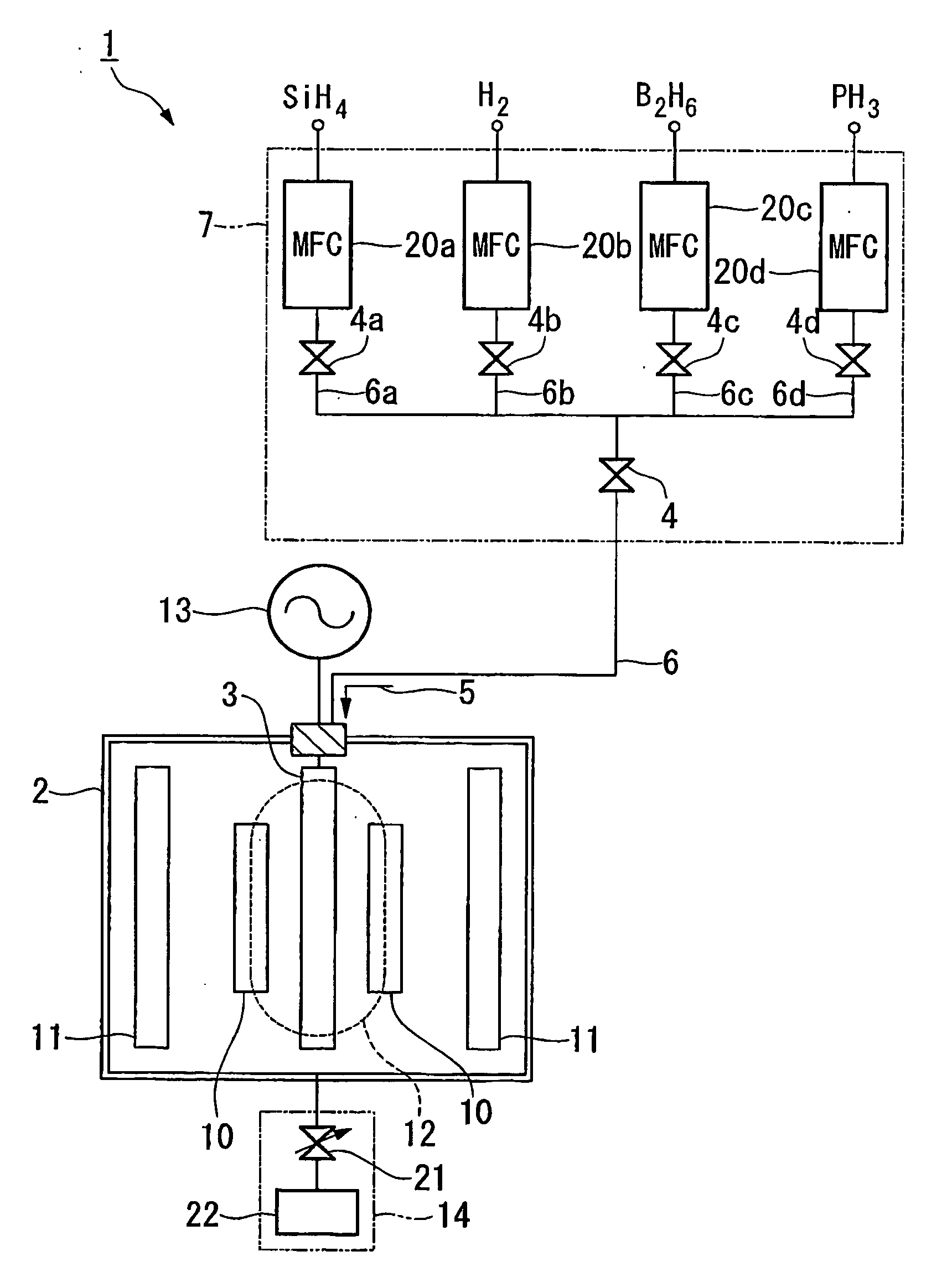
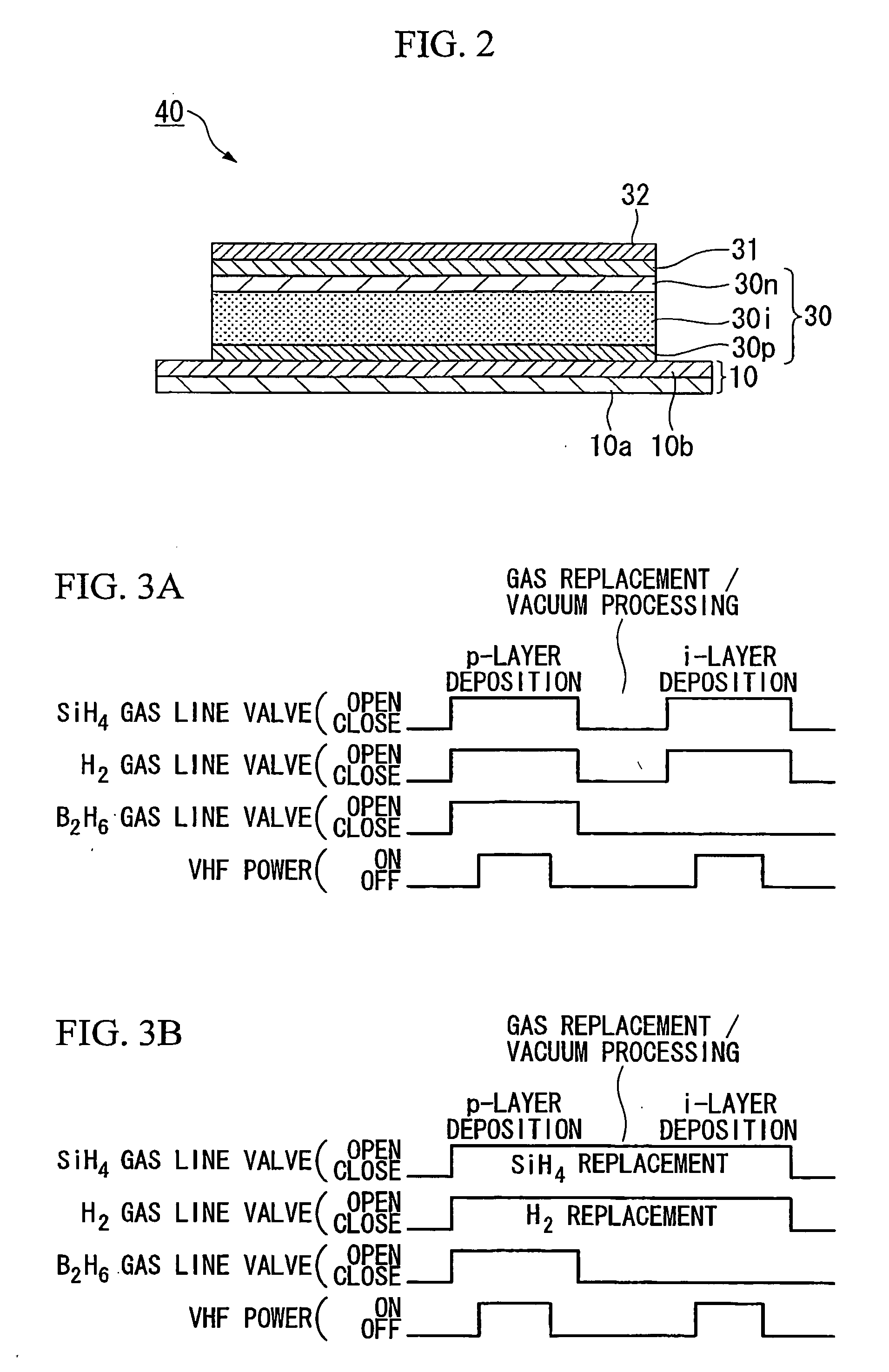
[0037] Hereunder, embodiments of the present invention will be described, with reference to the drawings. FIG. 1 is a block diagram showing one of the embodiments of a structure of an apparatus for forming thin films of the present invention. FIG. 2 is a cross-section showing an embodiment of a solar cell formed by the apparatus for forming thin films of the present invention.

[0038] As shown in FIG. 1, an apparatus for forming thin films 1 according to this embodiment is provided with a chamber 2, a U-shaped antenna 3 provided inside the chamber 2, a gas line 6 which supplies material gases 5 to the chamber 2 via a valve 4, a gas flow control apparatus 7 which controls opening and closing of the valve 4 to supply the material gases 5 to the chamber 2, a heating apparatus 11 which heats a substrate 10 arranged inside the chamber 2, a radio frequency power source 13 which generates a plasma 12 in the vicinity of the U-shaped antenna 3 in the chamber 2, and an exhaust apparatus 14 whi...


PUM

PropertyMeasurementUnit
Semiconductor propertiesaaaaaaaaaa

Abstract

An apparatus for forming thin films forms a plurality of thin films in a single chamber by sequential formation of at least a first and a second thin film on a substrate by an antenna type plasma CVD method. This apparatus is provided with a residual material removal apparatus, which removes from the chamber residual materials resulting from the step for forming the first film and which affect the properties of the second film. A method and an apparatus for forming films and a solar cell removes residual material (including material gas) resulting in the step for forming the first film which have an effect on the properties of the second film. Since a plurality of films are deposited inside a single chamber, it is unnecessary to provide a plurality of chambers, thus enabling the apparatus and solar cell to be more compact and of reduced cost.

Description

BACKGROUND OF THE INVENTION [0001] 1. Field of the Invention [0002] The present invention is a technique relating to a method for forming thin films, an apparatus for forming thin films and a solar cell, and in particular is used in a process for manufacturing a solar cell. [0003] 2. Description of Related Art [0004] Structures consisting of deposited films are sometimes used as a solar cell. In a structure, a p-type semiconductor thin film, an intrinsic semiconductor thin film (i-type semiconductor thin film), and an n-type semiconductor thin film are deposited, in the above order or in reverse order, on a substrate formed by a transparent conductive film. Conventionally, a parallel plate in-line plasma CVD apparatus is used for formation of a semiconductor layer. In this type of plasma CVD apparatus, the substrates are held on a grounded electrode, and material gases and RF power are supplied from a counter electrode. The each electrodes has approximately the same surface area as ...

Claims


Application Information

Patent Timeline
IPC IPC(8): C23C16/00C23C16/24C23C16/44C23C16/505H01L21/205H01L31/04H05H1/24
CPCC23C16/24H01J37/32082C23C16/505C23C16/45523
Inventor UEDA, MASASHITAKAGI, TOMOKOITO, NORIKAZU
Owner IHI CORP
Why Eureka
Try Eureka