Electron-emitting device manufacturing method, electron source manufacturing method, image-forming apparatus manufacturing method, and information displaying and playing apparatus manufacturing method
a manufacturing method and electron source technology, applied in the manufacture of electric discharge tubes/lamps, discharge tubes luminescnet screens, instruments, etc., can solve the problems of increasing cost, increasing cost, and difficult to uniformly control the length and shape of each carbon fiber located on the cathode electrode, so as to improve the electron emission characteristic, improve the stability and preferable electron emission characteristic, the effect of suppressing the effect of waste power consumption in driving
- Summary
- Abstract
- Description
- Claims
- Application Information
AI Technical Summary
Benefits of technology
Problems solved by technology
Method used
Image

Examples
embodiment 1
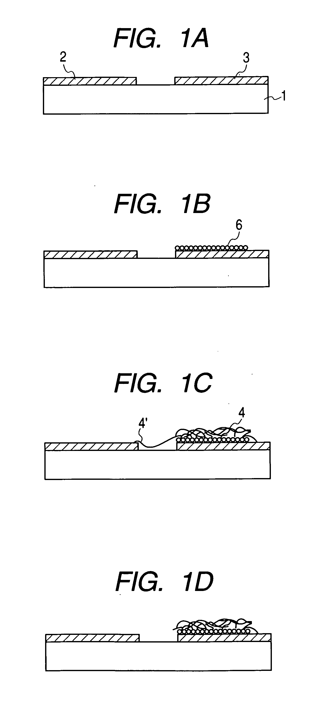
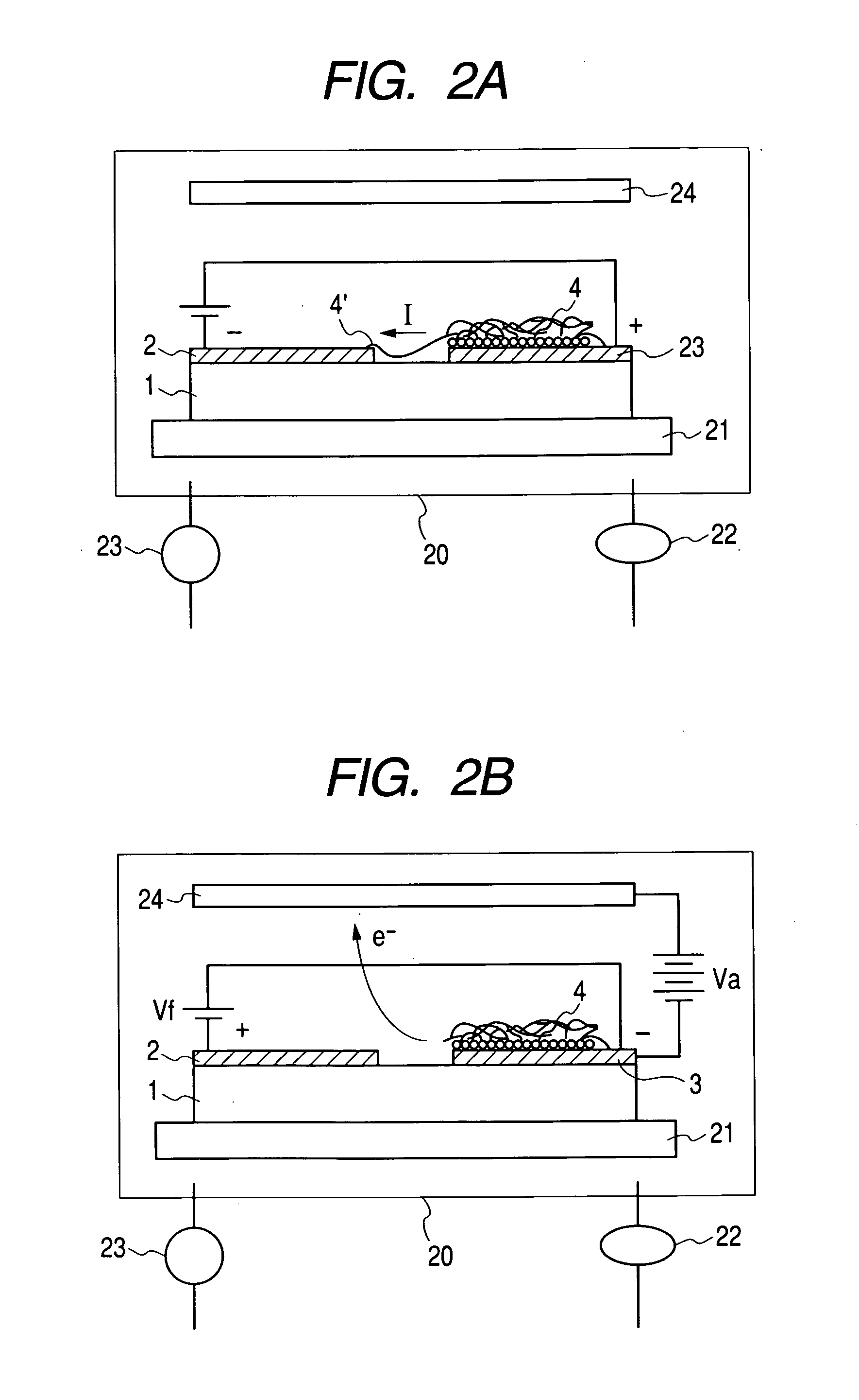
[0152] An example in which a carbon fiber that causes short-circuit is removed by applying a voltage having polarity reverse to that in driving between the first electrode and second electrode of an electron-emitting device is described as Embodiment 1.
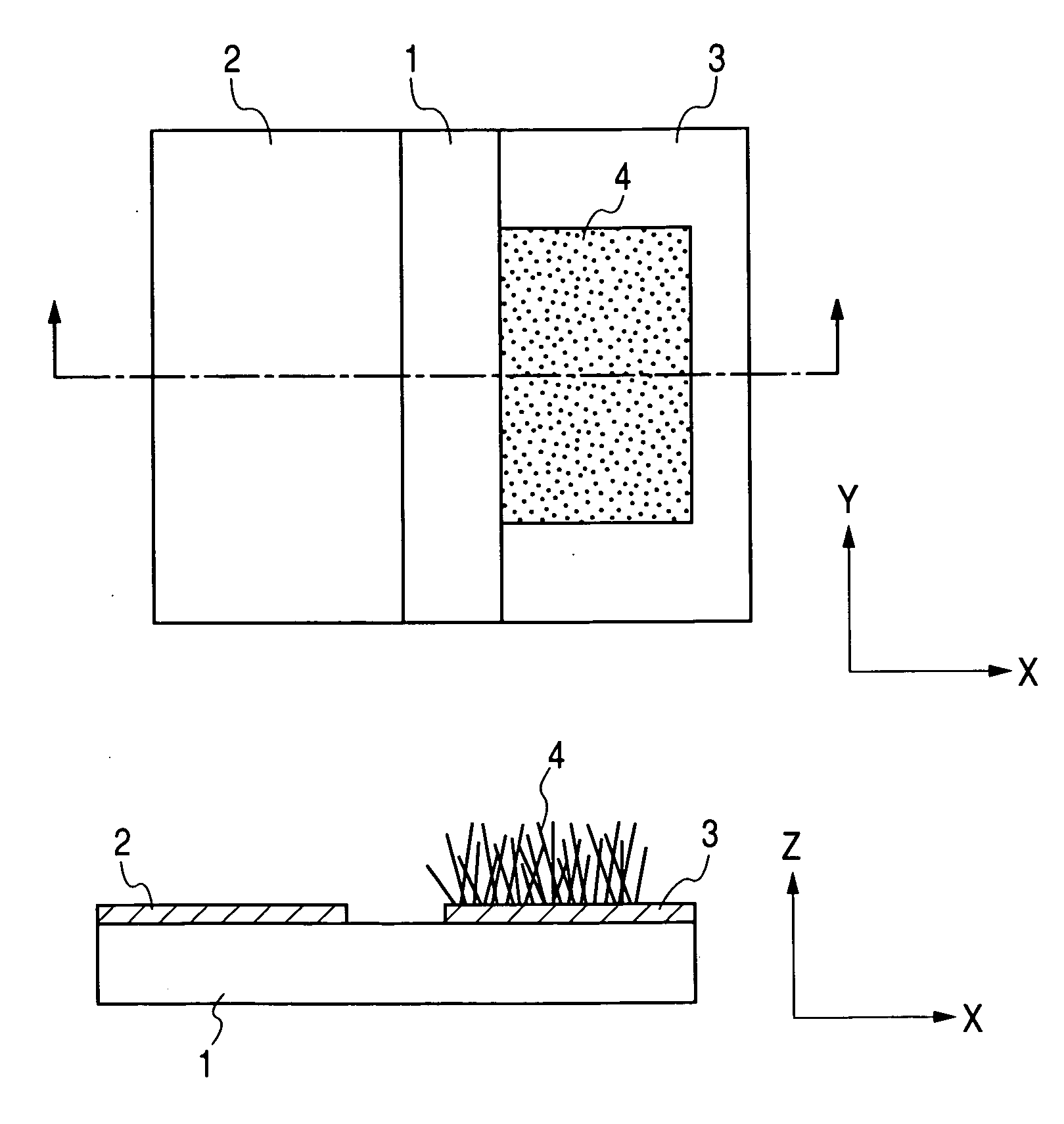
[0153]FIGS. 3A and 3B are the plan view and cross sectional view of an electron-emitting device manufactured in this embodiment. Hereinafter, steps of manufacturing the electron-emitting device according to this embodiment will be described in detail with reference to FIGS. 1A to 1D.
[0154] (First Step)
[0155] A quartz substrate was used as the substrate 1 and sufficiently washed. After that, a Ti layer having a thickness of 5 nm and a Pt layer having a thickness of 30 nm were successively formed as the first electrode 3 and the second electrode 2, respectively, by means of a sputtering method.
[0156] Next, a resist pattern was formed by means of a photo lithography process using a positive type photo resist. Then, the Pt layer and t...
embodiment 2
[0169] In Embodiment 2, an image display apparatus was manufactured using an matrix electron source produced by connecting a plurality of electron-emitting devices with a plurality of X-directional wirings and a plurality of Y-directional wirings. In this embodiment, an example in which the removal step was performed for each X-directional wiring will be described with reference to FIGS. 6 and 7.
[0170] In this embodiment, the X-directional wirings 62 were 400 wirings. Each of the wirings formed by means of an evaporation method had a thickness of about 1 μm and a width of 300 μm and contained Ag as a main component. The Y-directional wirings 63 were 600 wirings, each of which had a thickness of about 0.5 μm and a width of 100 μm and was formed by the same manner as that for the X-directional wirings 62. The interlayer insulating film which was not shown was provided at the intersections between the X-directional wirings 62 and the Y-directional wirings 63 and electrically insulated...
embodiment 3
[0180] An example in which the removal step was performed on only an electron-emitting device in which short-circuit occurs in a display apparatus serving as an image-forming apparatus including the matrix electron source on which the plurality of electron-emitting devices in Embodiment 2 were arranged will be described in this embodiment.
[0181] The electron source shown in FIG. 6 was manufactured as in Embodiment 2. Even in this embodiment, the Y-directional wiring 63 was connected with the cathode electrode and the X-directional wiring 62 was connected with the control electrode.
[0182] The electron source was manufactured by the same manufacturing method as that in Embodiment 1 and had the same structure as that in Embodiment 1. Note that the step of removing the carbon fiber that caused short-circuit was not performed. A current-voltage characteristic of each of the electron-emitting devices in such an electron source was measured. As a result, a leak current which might be cau...
PUM
| Property | Measurement | Unit |
|---|---|---|
| angle | aaaaa | aaaaa |
| angle | aaaaa | aaaaa |
| distance | aaaaa | aaaaa |
Abstract
Description
Claims
Application Information