Method of making substrates for nitride semiconductor devices

a technology of nitride semiconductors and substrates, which is applied in the direction of crystal growth process, polycrystalline material growth, chemically reactive gases, etc., can solve the problems of inconvenient large difference in linear expansion coefficient, easy dislocation of nitride semiconductor regions, and difficult to solve. , to achieve the effect of less cost and simplified process

Active Publication Date: 2005-06-02
SANKEN ELECTRIC CO LTD
View PDF0 Cites 46 Cited by
  • Summary
  • Abstract
  • Description
  • Claims
  • Application Information

AI Technical Summary

Benefits of technology

[0009] The present invention seeks to provide a greatly simplified and less costly method of creating a substrate system including a nitride semiconductor region having dislocations reduced to a minimum, without the difficulties heretofore encountered in the art.
[0012] Thus the present invention has succeeded in creating interstices in the first layer without relying upon the masking or metal vaporizing process needed by the prior art. As the third layer is formed by vapor-phase epitaxy in mating engagement with the intersticed first layer, dislocation density is reduced in this third layer on the same principle as in the aforesaid Japanese Unexamined Patent Publication Nos. 10-312971 and 2002-343728. The fabrication of semiconductor systems having the nitride semiconductor third layer of reduced dislocations is thus made easier and less costly and time-consuming than heretofore.

Problems solved by technology

There have been difficulties left unresolved with the semiconductor substrates of the prior art construction outlined above.
The silicon baseplate or substrate proper and the nitride semiconductor region thereon have an inconveniently great difference in coefficient of linear expansion, such that dislocations were easy to occur in the nitride semiconductor region.
Too many dislocations taking place in the nitride semiconductor region led to such deficiencies in performance as a drop in the efficiency of light emission (in the case of an LED) and a rise in current leakage.
This approach is still unsatisfactory because of the costs and labor associated with the production of the mask.
This approach is also objectionable by reason of the complex and costly method of manufacture involving use of the two different fabrication processes of epitaxy and vapor deposition.

Method used


Image

  • Method of making substrates for nitride semiconductor devices
  • Method of making substrates for nitride semiconductor devices
  • Method of making substrates for nitride semiconductor devices

Examples


Embodiment Construction

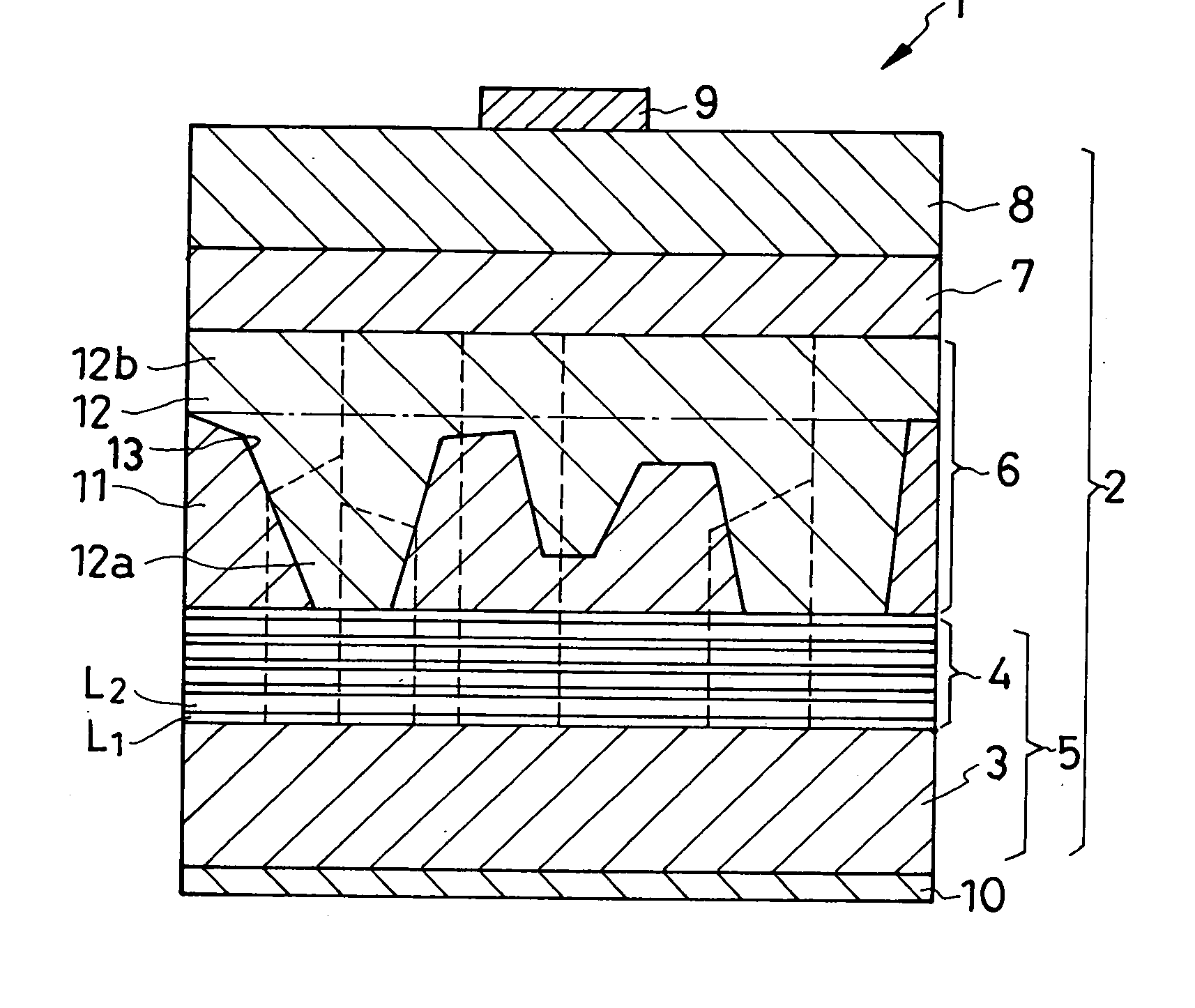
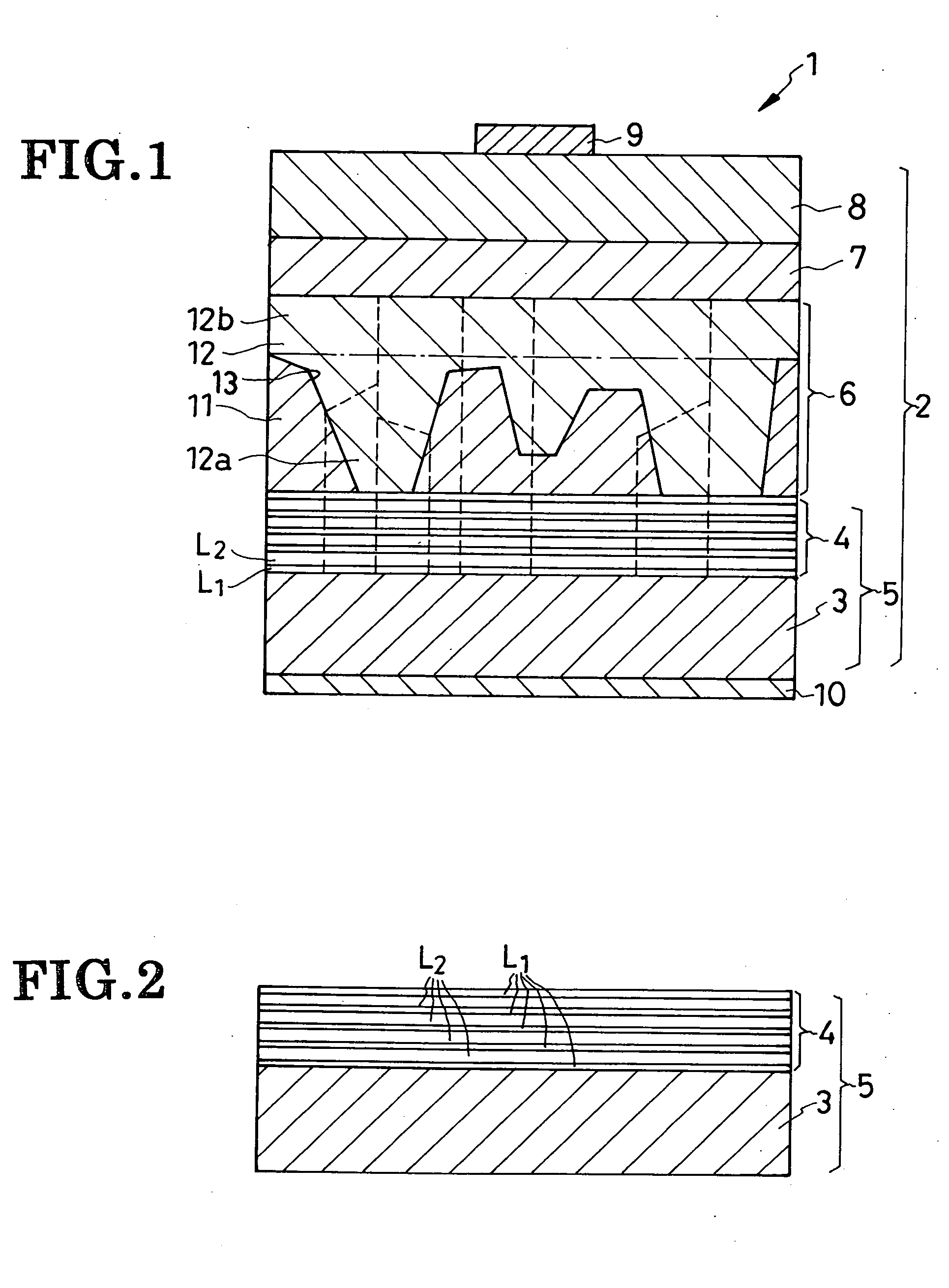
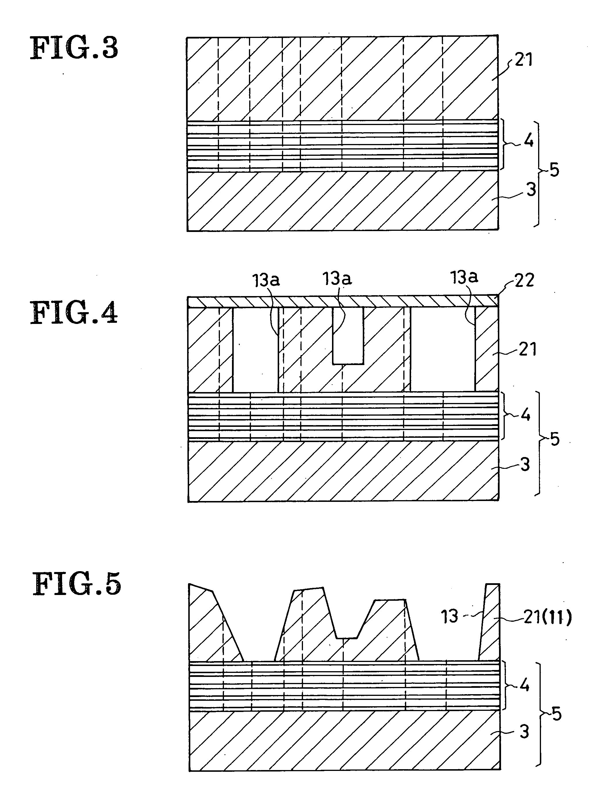
[0026] The method of this invention will now be described more specifically as adapted for the fabrication of the LED 1 shown in FIG. 1. FIGS. 2-7 show successive steps in the course of the fabrication of the LED 1 and will be referred to more specifically during the subsequent description of the method of making the LED. The LED 1 has an LED body or LED substrate system 2 constituting part of a wafer which is sized for joint production of a plurality or multiplicity of LEDs.

[0027] The LED substrate system 2 includes a baseplate 3 which, in combination with an overlying buffer region 4, constitutes a baseplate system 5. Overlying this baseplate system 5 are three main semiconductor layers 6, 7 and 8, arranged one on top of another in that order from the lowermost one upward. The lowermost main semiconductor layer 6 is an n-type cladding or confining layer; the intermediate main semiconductor layer 7 is an active layer; and the topmost main semiconductor layer 8 is a p-type cladding...


PUM

PropertyMeasurementUnit
thickaaaaaaaaaa
thickaaaaaaaaaa
thickaaaaaaaaaa

Abstract

For fabricating an LED substrate with minimal dislocations in its nitride semiconductor layers, GaN is epitaxially grown into a first formative layer overlying a multilayered buffer region on a silicon substrate. A second formative layer is then formed on the first formative layer by epitaxially growing AlN, at such a rate that interstices are created in the first formative layer by the etching action of the reactor gases in the early stages of the fabrication of the second formative layer. Then the second formative layer is etched away from over the intersticed first formative layer, leaving the interstices open. Then a filler layer of GaN is epitaxially grown on the intersticed first formative layer in interfitting engagement therewith. Dislocations are greatly reduced in active semiconductor layers formed subsequently on the filler layer.

Description

CROSS REFERENCE TO RELATED APPLICATIONS [0001] This application claims priority to Japanese Patent Application No. 2003-398669, filed Nov. 28, 2003. BACKGROUND OF THE INVENTION [0002] This invention relates to a method of making semiconductor substrates for production of nitride semiconductor devices. The semiconductor substrates made by the method of the invention are currently believed to be best suited for production of light-emitting diodes (LEDs), high-electron-mobility transistors (HEMTs), and field-effect transistors (FETs), among other devices. [0003] Nitride semiconductor devices are formed on semiconductor substrates or dice cut from a wafer. Each such substrate comprises a baseplate or substrate proper of either sapphire, silicon carbide, or silicon, and a lamination or of nitride semiconductor layers grown epitaxially on the baseplate. Of the listed baseplate materials, sapphire and silicon carbide are so expensive that silicon is now used preferentially, as taught in Ja...

Claims


Application Information

Patent Timeline
Patent Type & Authority Applications(United States)
IPC IPC(8): C30B25/02C30B29/40H01L21/20H01L21/205C30B29/38H01L21/335H01L21/338H01L29/20H01L29/778H01L29/812H01L33/06H01L33/12H01L33/32H01L33/34
CPCC30B25/02C30B29/40H01L21/0237H01L21/02458H01L21/02505H01L33/007H01L21/0262H01L21/02658H01L29/2003H01L29/66462H01L21/0254
Inventor OTSUKA, KOJISATO, JUNJISUGAHARA, TOMOYA
Owner SANKEN ELECTRIC CO LTD
Why Eureka
Try Eureka