
Method for cutting liquid crystal display panel

Active Publication Date: 2005-06-02
LG DISPLAY CO LTD
View PDF39 Cites 20 Cited by
  • Summary
  • Abstract
  • Description
  • Claims
  • Application Information

AI Technical Summary

Benefits of technology

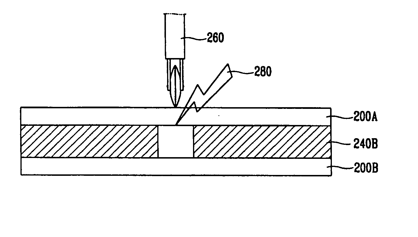
[0019] An object of the present invention is to provide a method for cutting a liquid crystal display panel that before forming a scribe line, removes a portion of a seal line that would overlap a scribe line if not removed, thereby ensuring smooth breakage between unit liquid crystal display panels and increasing a fabrication yield.

Problems solved by technology

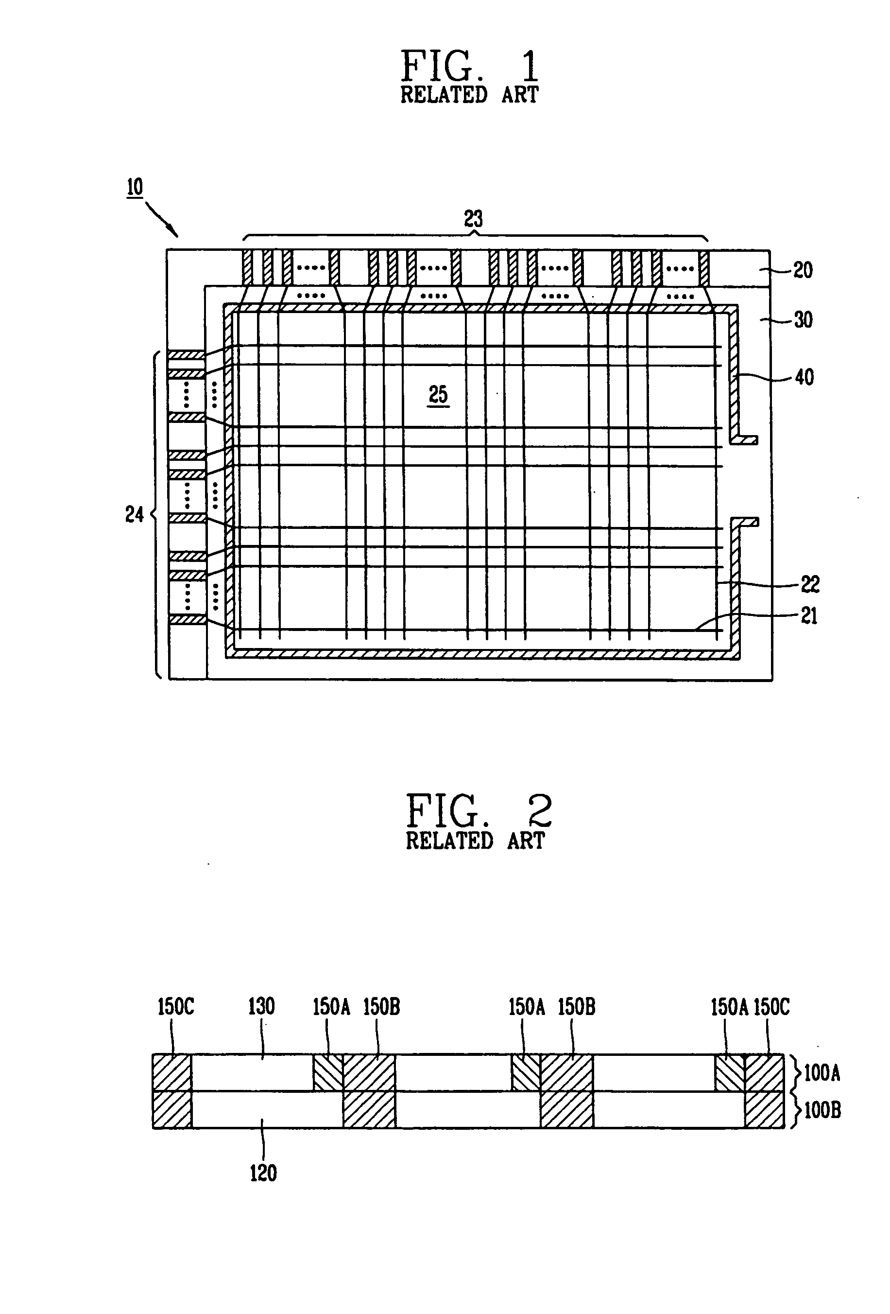
However, the cutting process is not smoothly performed at the seal pattern 140.
Because a scribe line is formed only on the first mother substrate 100A, when a breaking process is performed, vertical or horizontal cracks are undesirably generated at a portion where the seal line is overlapped with the scribing line.
As a result, the substrates cannot be properly cut or the cut sectional side becomes rough.
When this happens, the substrate should be discarded, thereby reducing a fabrication yield.

Method used


Image

  • Method for cutting liquid crystal display panel
  • Method for cutting liquid crystal display panel
  • Method for cutting liquid crystal display panel

Examples


Embodiment Construction

[0032] Reference will now be made in detail to the preferred embodiments, examples of which are illustrated in the accompanying drawings.

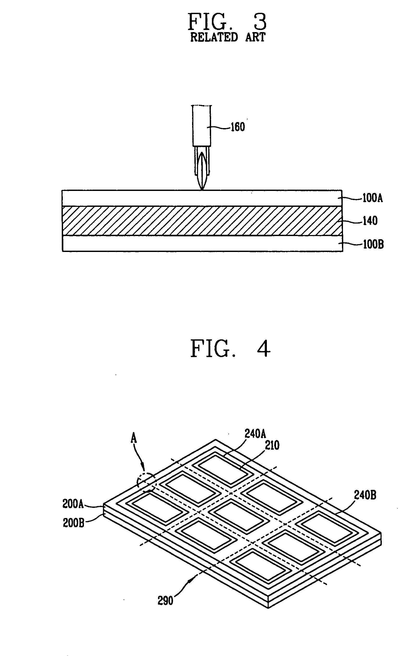
[0033]FIG. 4 is a perspective view of mother substrates according to an embodiment of the present invention. In FIG. 4, a first mother substrate 200A and a second mother substrate 200B may be attached to each other by first and second seal patterns 240A and 240B. The first mother substrate 200A may include a plurality of unit color filter substrates and the second mother substrate 200B may include a plurality of unit array substrates. In addition, a liquid crystal layer (not shown) may be formed between the first and second mother substrates 200A and 200B. Accordingly, the first and second mother substrates 200A and 200B may be cut and broken along scribe lines 290 to form a plurality of unit liquid crystal display panels 210.

[0034] The liquid crystal layer (not shown) may be formed by a liquid injection method and a liquid dropping method. When ...


PUM

PropertyMeasurementUnit
Timeaaaaaaaaaa
Pressureaaaaaaaaaa

Abstract

A method for cutting a liquid crystal display panel includes providing first and second mother substrates, forming a scribing line on the first and second mother substrates, removing a portion of a seal line being overlapped with the scribing line, the seal line formed on one of the first and second mother substrates, and dividing the first and second mother substrates into a plurality of unit liquid crystal display panels along the scribing line.

Description

[0001] The present application claims the benefit of Korean Patent Application No. 10-2003-86032 filed in Korea on Nov. 29, 2003, which is hereby incorporated by reference. BACKGROUND OF THE INVENTION [0002] 1. Field of the Invention [0003] The present invention relates to a method for cutting a substrate, and more particularly, to a method for cutting a liquid crystal display panel fabricated on a large-sized mother substrate into individual liquid crystal display panel units that avoid panel degradation caused by a seal pattern. [0004] 2. Discussion of the Related Art [0005] Image display devices have become increasingly important in the current Information Age and demands for image display devices that have high resolution images, lightness, thin profile, compact size, and low voltage power consumption are growing. Presently, a liquid crystal display (LCD), which is a major product of a flat panel display (FPD), that meets such demands is available for mass production as a substi...

Claims


Application Information

Patent Timeline
IPC IPC(8): B23K26/364B28D5/00G02F1/1333G02F1/13G02F1/1335G02F1/1339
CPCG02F1/133351G02F1/13
Inventor JUNG, SUNG SU
Owner LG DISPLAY CO LTD
Learn More