Single-crystal silicon ingot and wafer having homogeneous vacancy defects, and method and apparatus for making same

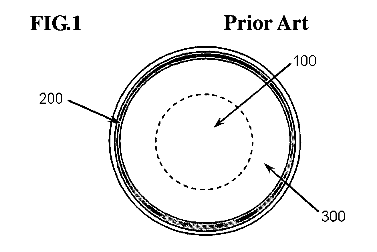
a single crystal silicon, homogeneous technology, applied in the direction of silicon compounds, under a protective fluid, transportation and packaging, etc., can solve the problems of coarse vacancy defects, adversely affecting the voltage-resistance characteristics of single crystal silicon, and coarse vacancy defects at the center part, etc., to achieve high quality and low defect

Active Publication Date: 2005-06-09
LG SILTRON
View PDF4 Cites 16 Cited by
  • Summary
  • Abstract
  • Description
  • Claims
  • Application Information

AI Technical Summary

Benefits of technology

[0026] The present invention improves upon the Czochralski (CZ) method of manufacturing single-crystal silicon ingots, and provides a method of manufacture, an apparatus for single-crystal silicon ingot and wafer production; and high quality, low defect, single-crystal silicon ingots and wafers.

Problems solved by technology

Furthermore, coarse-vacancy defects, such as crystal originated particles (COP) or flow pattern defects (FPD), exist in the ingot interior since the value of G increases as one moves from the center of the ingot to the circumferential edge of the ingot.
There has been effort to remove or reduce crystal originated particles (COP), which adversely affect the voltage-resistance characteristics of the single crystal silicon.
As shown in FIG. 1, if the ingot is grown in the pulling direction such that the oxidation-induced stacking fault ring exists at the typical hot zone, coarse vacancy defects are formed at the center part of the ingot due to heat accumulation and slow cooling effects.
Since the cooling speed in the region between the exterior of the center part and the interior of the oxidation-induced staking fault ring is faster than that at the center part of the ingot, micro-vacancy defects are formed, and the vacancy defects are not uniformly distributed in the radial direction.
Also, the micro-vacancy defects formed due to fast cooling deteriorate the voltage-resistance characteristic of the oxide layer, and this occurs around the exterior circumferential part of the wafer at which the rate of cooling is relatively high.
However, lowering the pulling speed causes a loss in productivity, and excessive reduction of the pulling speed is likely to, increase the formation of interstitial defects.

Method used


Image

  • Single-crystal silicon ingot and wafer having homogeneous vacancy defects, and method and apparatus for making same
  • Single-crystal silicon ingot and wafer having homogeneous vacancy defects, and method and apparatus for making same
  • Single-crystal silicon ingot and wafer having homogeneous vacancy defects, and method and apparatus for making same

Examples


Embodiment Construction

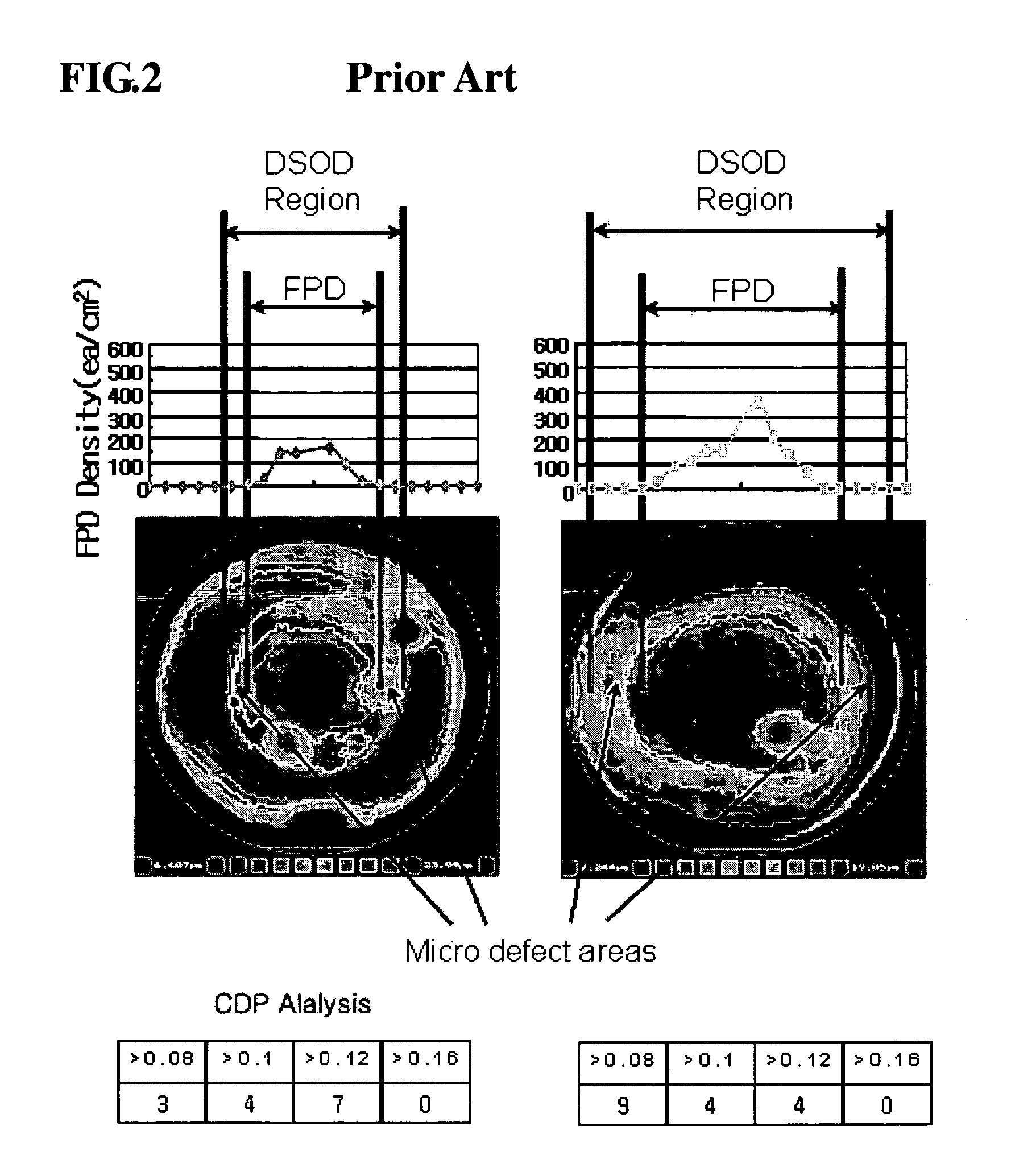
[0050] The present invention enhances the voltage-resistance characteristic of an oxide layer in the single-crystal silicon grown by the Czochralski (CZ) method by growing a single-crystal silicon ingot in a manner whereby each micro defect is smaller than the critical size that adversely affects the voltage-resistance characteristic of an oxide layer (typically 0.065 microns), and each coarse defect larger than the critical size is distributed in the radial direction.

[0051] The voltage-resistance characteristic of an oxide layer of the device fabricated on the single crystal silicon substrate can be represented by the tolerable voltage and time before the silicon oxide layer formed on the silicon wafer is destructed and the insulating property of the silicon oxide layer is disappeared.

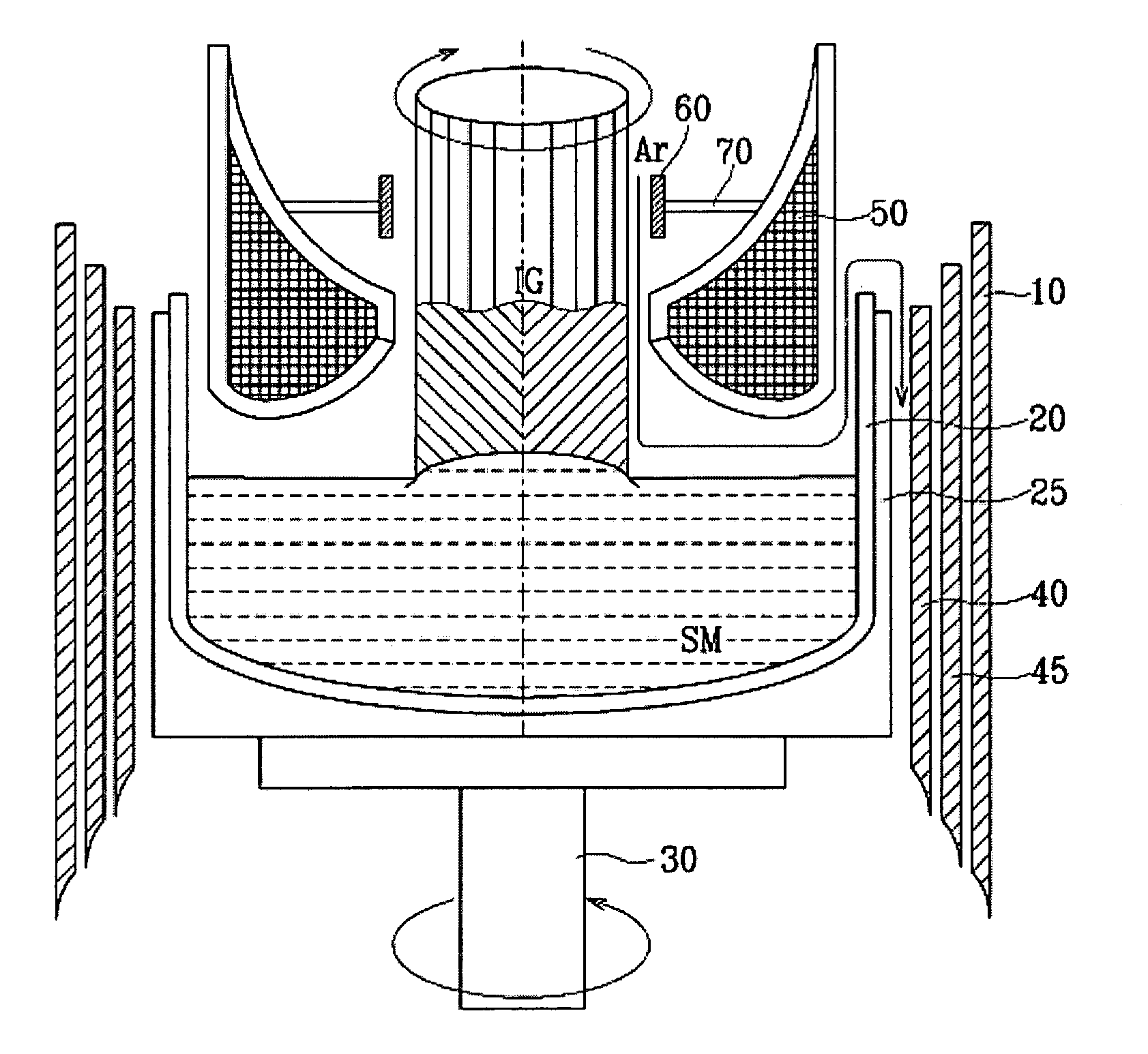
[0052] In one embodiment of the invention, the outer circumferential part of the ingot is cooled faster than the center part is cooled, and the thermal history of the ingot is uniformly distributed ...


PUM

PropertyMeasurementUnit
temperatureaaaaaaaaaa
sizeaaaaaaaaaa

Abstract

The present invention improves upon the Czochralski method for growing a single-crystal silicon ingot and provides a high quality silicon wafer having an oxide layer with superior voltage-resistance characteristics. An apparatus and method are also provided, whereby vacancy defect density and distribution are uniformly controlled. A single-crystal silicon ingot is grown under a condition where the temperature variation of the ingot is less than or equal to 20° C./cm in the temperature range of 1000 to 1100° C.

Description

CROSS-REFERENCE TO RELATED APPLICATION [0001] This application claims priority of Korean Patent Application Nos. 10-2003-0087179 and 10-2003-0087180, each filed Dec. 3, 2003, the entire disclosures of which are incorporated herein by reference. BACKGROUND OF THE INVENTION [0002] (a) Field of the Invention [0003] The present invention relates to a method for growing a single-crystal silicon ingot based on the Czochralski method, and more particularly to an apparatus and method for growing the single-crystal silicon ingot while maintaining a uniform growing condition and cooling condition in a radial direction of the ingot; and the single-crystal silicon ingot and wafers produced therefrom, having uniform vacancy defects in a radial direction. [0004] (b) Description of the Related Art [0005] The voltage-resistance characteristic of an oxide layer of a semiconductor device fabricated from a single-crystal silicon substrate can be represented by the tolerable voltage and time before the...

Claims


Application Information

Patent Timeline
Patent Type & Authority Applications(United States)
IPC IPC(8): C30B15/14C30B15/20C30B29/06
CPCC30B15/14Y10T428/21C30B29/06C30B15/20
Inventor HONG, YOUNG HOCHOI, ILL SOOKIM, SANG HEEKWAK, MAN SEOKLEE, HONG WOO
Owner LG SILTRON
Why Eureka
Try Eureka