
Method and apparatus for decomposing semiconductor device patterns into phase and chrome regions for chromeless phase lithography

a semiconductor device and lithography technology, applied in the field of methods, can solve the problems of reducing the size of an integrated circuit, cd (critical dimension) of the corresponding mask pattern approaching the resolution limit of the optical exposure tool, and long, tedious and difficult processes, so as to reduce the time required for mask design and improve the accuracy of the design printed

Active Publication Date: 2005-06-09
ASML NETHERLANDS BV
View PDF37 Cites 9 Cited by
  • Summary
  • Abstract
  • Description
  • Claims
  • Application Information

AI Technical Summary

Benefits of technology

This method simplifies the mask design process, reduces time required for mask generation, and enhances the accuracy of the printed pattern on the wafer, enabling the printing of smaller features beyond current resolution limits.

Problems solved by technology

These rules are set by processing and design limitations.
As the size of an integrated circuit is reduced and its density increases, however, the CD (critical dimension) of its corresponding mask pattern approaches the resolution limit of the optical exposure tool.
However, due to the complexity of the masks, this can be a long, tedious and difficult process.

Method used


Image

  • Method and apparatus for decomposing semiconductor device patterns into phase and chrome regions for chromeless phase lithography
  • Method and apparatus for decomposing semiconductor device patterns into phase and chrome regions for chromeless phase lithography
  • Method and apparatus for decomposing semiconductor device patterns into phase and chrome regions for chromeless phase lithography

Examples


Embodiment Construction

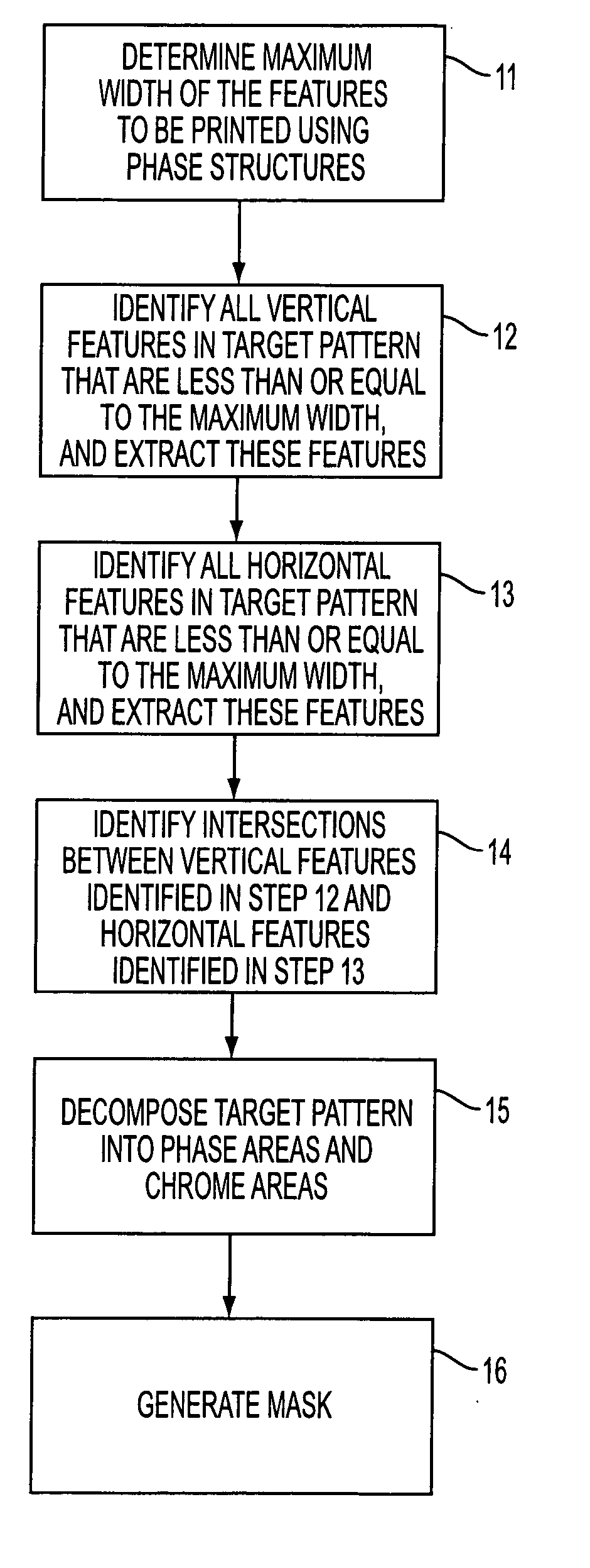
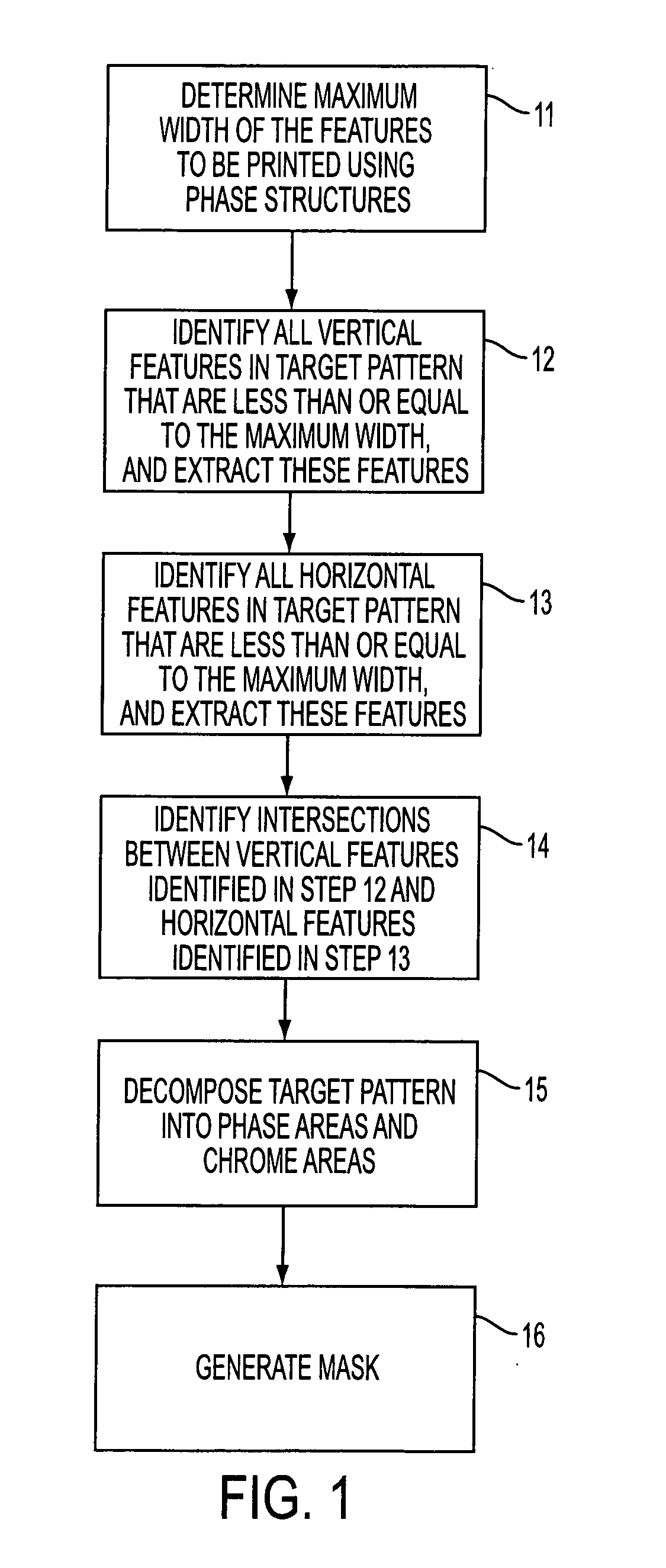
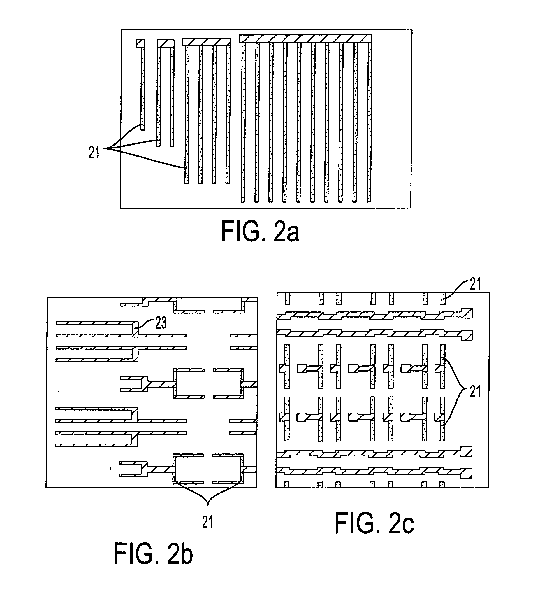
[0027] As explained in more detail below, the preferred embodiment of the present invention relates to a process for decomposing a desired target pattern (to be printed on a wafer) so as to produce a mask pattern (i.e., reticle) that can be utilized to image the wafer / substrate and generate the target pattern thereon. In accordance with the present invention, the mask pattern to be generated utilizes CPL techniques. As such, the mask pattern will include areas that are approximately 100% transmission and zero phase shift; areas that are approximately 100% transmission and 180° phase-shift; and areas that are approximately 0% transmission. Due to these various different types of areas utilized to print features when utilizing CPL techniques in combination with the complexity of typical masks, mask design can be a difficult and time extensive task. As explained in detail below, the present invention reduces the time required for mask generation by providing a simple decomposition proc...


PUM

PropertyMeasurementUnit
wavelengthaaaaaaaaaa

Abstract

A method of generating a mask of use in printing a target pattern on a substrate. The method includes the steps of (a) determining a maximum width of features to be imaged on the substrate utilizing phase-structures formed in the mask; (b) identifying all features contained in the target pattern having a width which is equal to or less than the maximum width; (c) extracting all features having a width which is equal to or less than the maximum width from the target pattern; (d) forming phase-structures in the mask corresponding to all features identified in step (b); and (e) forming opaque structures in the mask for all features remaining in target pattern after performing step (c).

Description

FIELD OF THE INVENTION [0001] The present invention relates generally to the generation of mask patterns for use with chromeless phase lithography techniques, and more specifically, for the decomposition of a target design into a corresponding mask pattern that prints features utilizing both chrome and phase-shift techniques. In addition, the present invention relates to a device manufacturing method using a lithographic apparatus comprising a radiation system for providing a projection beam of radiation; a mask table for holding a mask, serving to pattern the projection beam; a substrate table for holding a substrate; and a projection system for projecting the patterned projection beam onto a target portion of the substrate. BACKGROUND OF THE INVENTION [0002] Lithographic projection apparatus (tools) can be used, for example, in the manufacture of integrated circuits (ICs). In such a case, the mask contains a circuit pattern corresponding to an individual layer of the IC, and this ...

Claims


Application Information

Patent Timeline
Patent Type & Authority Applications(United States)
IPC IPC(8): G03F1/00G03F7/20H01L21/027
CPCG03F1/144G03F1/34G03F1/36G03F7/70941G03F7/70425G03F7/70466G03F7/70125H01L21/027
Inventor BROEKE, DOUG VAN DENCHEN, JANG FUNGLAIDIG, THOMASWAMPLER, KURT E.HSU, STEPHEN
Owner ASML NETHERLANDS BV
Learn More