Display device

a technology of display device and display screen, which is applied in the direction of discharge tube luminescnet screen, non-linear optics, instruments, etc., can solve the problems of display area and affect the display, and achieve the effects of reducing display area, increasing display value, and increasing valu

Inactive Publication Date: 2005-06-16
SEMICON ENERGY LAB CO LTD
View PDF16 Cites 21 Cited by
  • Summary
  • Abstract
  • Description
  • Claims
  • Application Information

AI Technical Summary

Benefits of technology

[0015] According to the invention, a narrower frame and suppression of a voltage drop of a lead wiring are realized by providing the lead wiring externally which conventionally occupied a large area in a frame region.
[0022] In this manner, by providing the lead wiring externally and supplying a voltage from the external connecting portion, at least a region of a substrate in which the external connecting portion is not formed can be narrowed. Thus, a display area can be reduced, a display can be increased, and an added value can be increased by mounting a circuit and the like having various functions.
[0026] In this manner, by removing the lead wiring to supply a voltage and utilizing a sealing can for sealing, at least a portion in which the lead wiring is conventionally formed can be narrowed. Thus, a display area can be decreased, a display can be increased, and an added value can be increased by mounting a circuit and the like having various functions. Moreover, the number of pins can be reduced since it is no longer necessary to supply a voltage to an anode line or a cathode line through an external connecting portion and a flexible wiring substrate (such as an FPC).
[0027] By applying a structure of the invention, a portion of a frame region which was conventionally occupied by the lead wiring can be used as a display region, which results in realizing a narrower frame. Further, wiring resistance can also be reduced, which reduces an adverse effect of a voltage drop and improves a display quality. According to the aforementioned effects, a display device which meets users' demands and has a high added value can be provided.

Problems solved by technology

This voltage drop being too large, a display could also be affected.

Method used


Image

  • Display device
  • Display device
  • Display device

Examples


embodiment mode 1

[0043] In this embodiment mode, an example of substituting a lead wiring by a flexible wiring substrate is described with reference to FIGS. 1A to 1C.

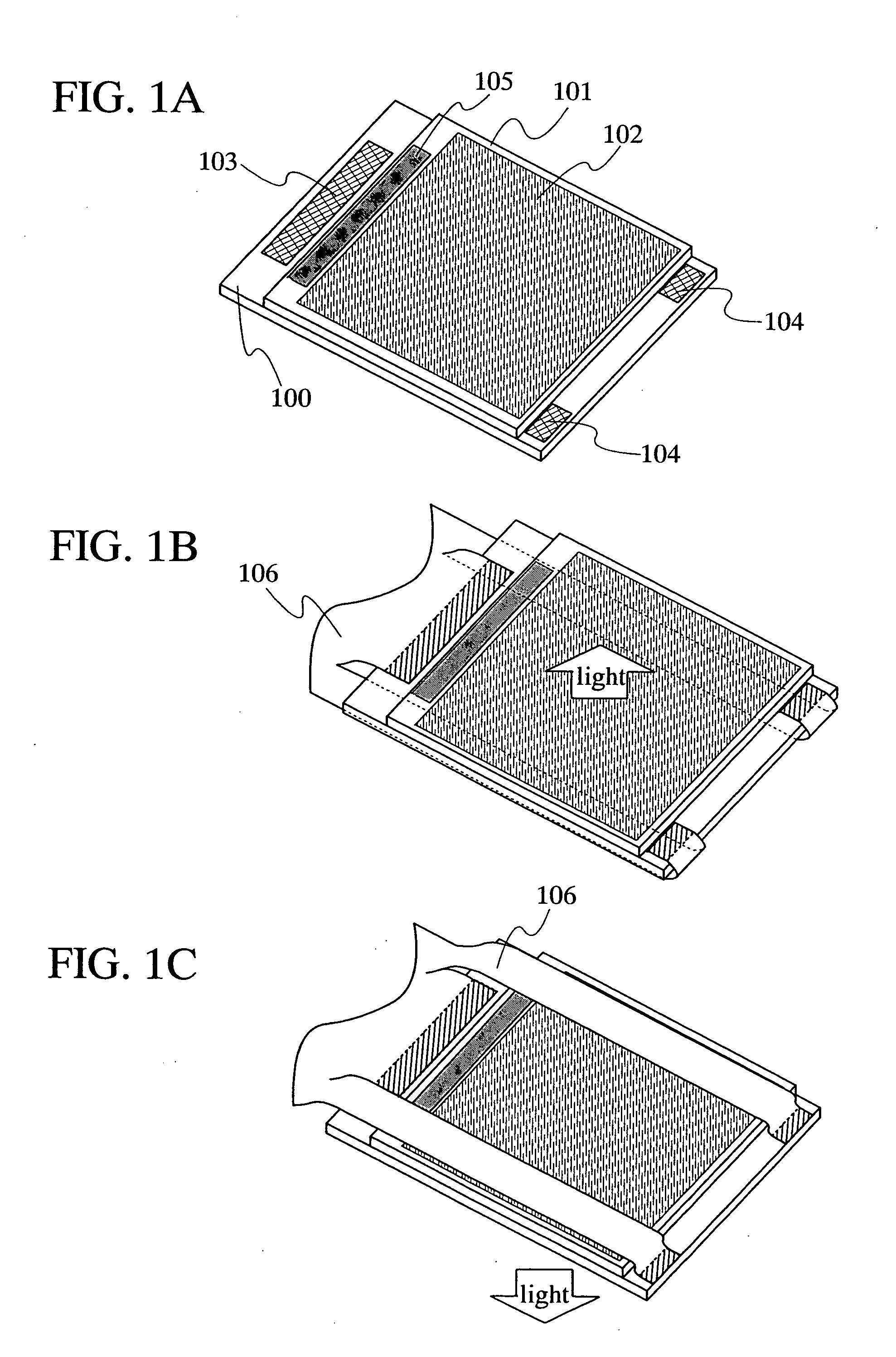
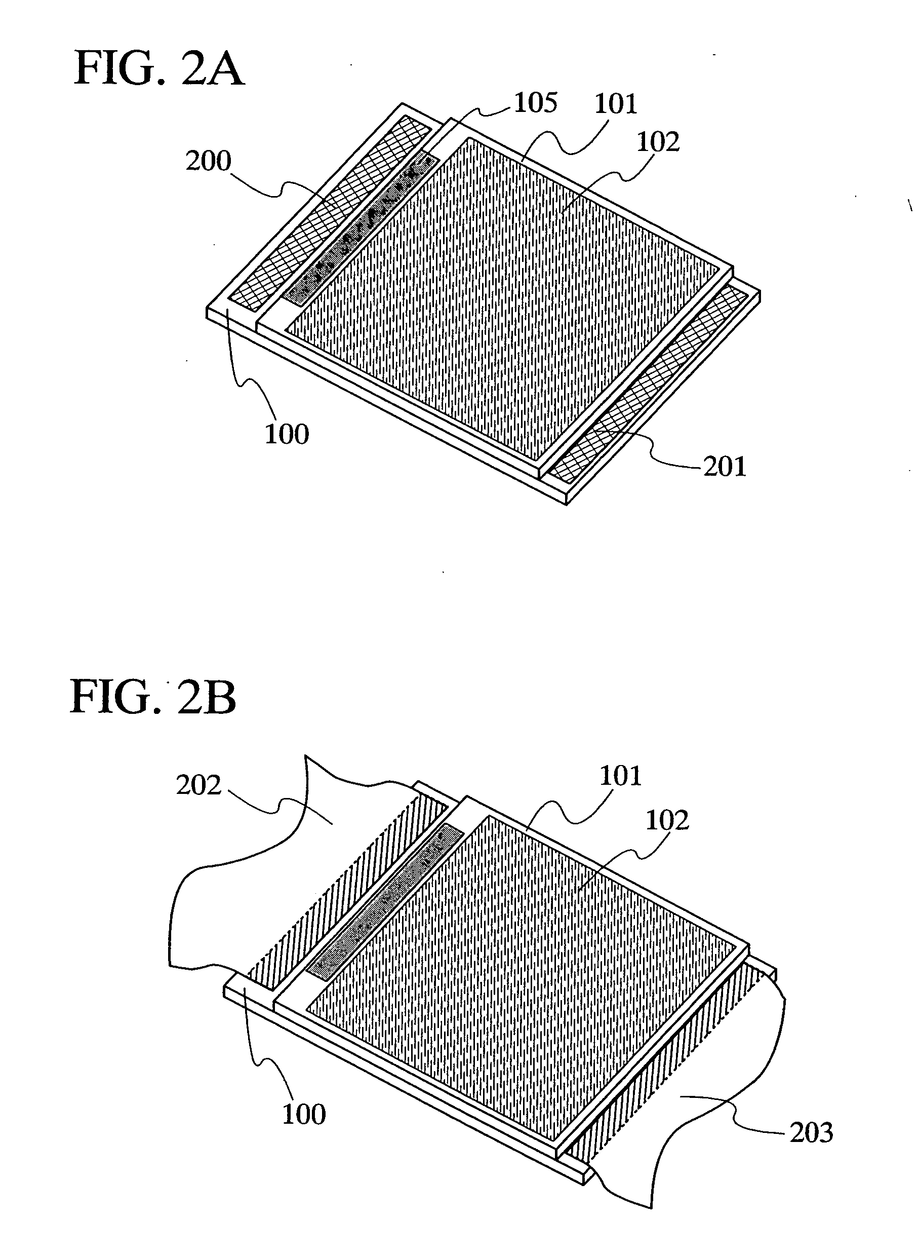
[0044] First, a conventional structure is described with reference to FIG. 11. Reference numeral 100 denotes a substrate, 101 denotes a counter (sealing) substrate, 102 denotes a display portion, 103 denotes an external connecting portion, 105 denotes a driver circuit portion, and 500 denotes a lead wiring. In this manner, the display portion 102 in the conventional structure is quite small relative to a substrate due to the lead wiring 500.

[0045]FIG. 1A shows a panel which is used for an electroluminescent display using the invention. The display portion 102 is formed by sealing electroluminescent elements formed on the substrate 100 with the counter substrate 101. Reference numerals 103 and 104 denote external connecting portions, and 105 denotes a driver circuit portion. Note that anode lines or cathode lines are formed in the dis...

embodiment mode 2

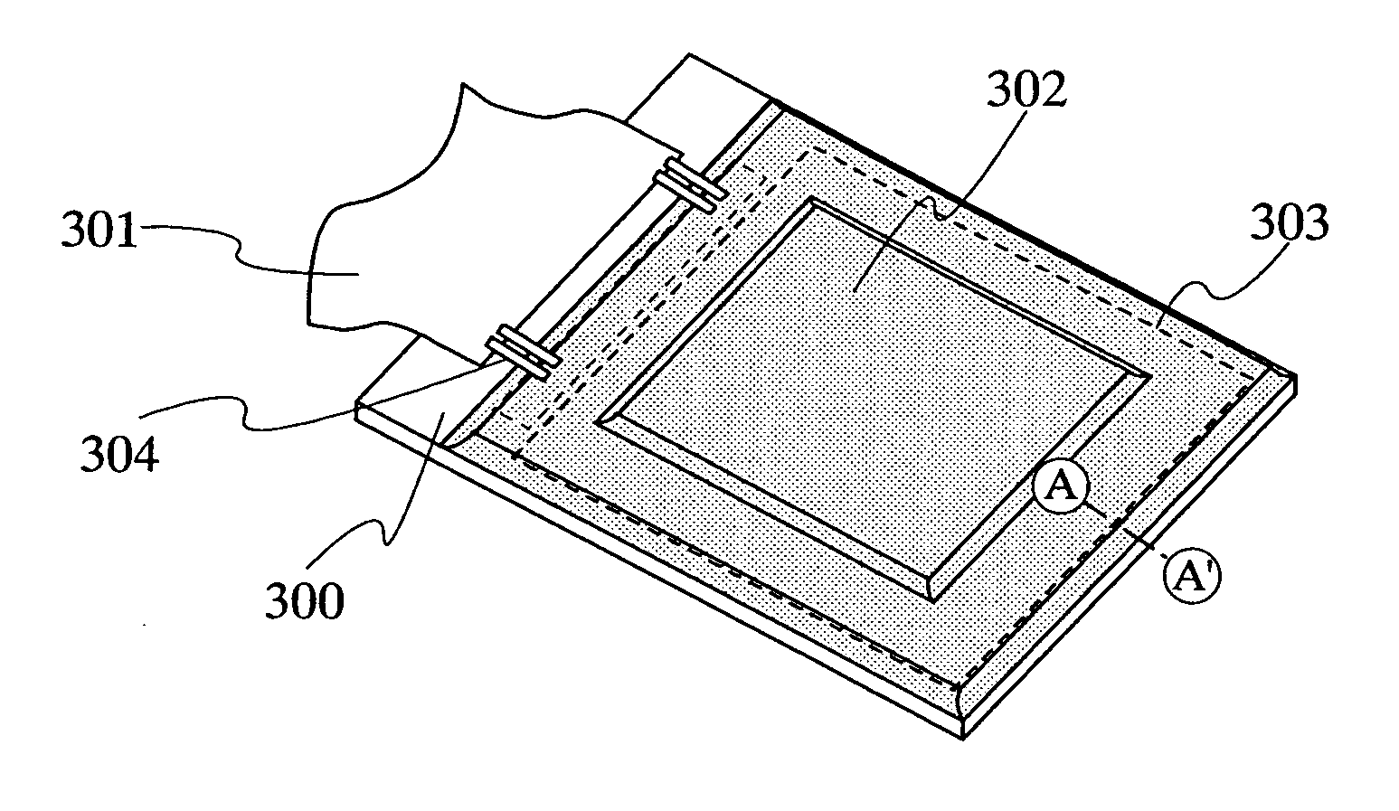
[0057] In this embodiment mode, an example of substituting the lead wiring by a sealing can is described with reference to FIGS. 3A to 3C.

[0058]FIG. 3A is a perspective view which realizes the structure of the invention by using a sealing can. A substrate 300, a flexible wiring substrate 301, a sealing can 302, a display portion 303, and a voltage supply portion 304 for the sealing can 302 are provided. In this structure, ends of the anode lines or the cathode lines on the flexible wiring substrate 301 side are supplied with a voltage from the flexible wiring substrate 301 and a voltage is supplied to the other ends thereof which are far from the flexible wiring substrate 301 through the sealing can.

[0059]FIGS. 3B and 3C are sectional views of a portion (A-A′ in the perspective view) in which a voltage is supplied from the sealing can 302 to the anode lines or the cathode lines. A driving transistor (P-channel type) for driving a light emitting element 313 is formed in a display r...

embodiment mode 3

[0065] In this embodiment mode, another structure of the invention is described with reference to FIGS. 6A and 6B. In this embodiment mode, an example of forming a conductive film as a substitute for a lead wiring on a counter substrate is described.

[0066] A counter substrate is used when sealing an element substrate over which electroluminescent elements are formed with a sealant such as an ultraviolet curing resin. The electroluminescent elements can be blocked from the outside air by being sealed with the sealant and the counter substrate, resulting in improved reliability.

[0067] In this embodiment mode, a conductive film is formed on the counter substrate as a substitute for the lead wiring, a voltage is supplied to the conductive film, and a voltage is supplied to anode lines or cathode lines by causing the conductivity between the conductive film and the anode lines or the cathode lines.

[0068] The conductive film formed on the counter substrate may have any shape, although ...


PUM

PropertyMeasurementUnit
thicknessaaaaaaaaaa
thicknessaaaaaaaaaa
thicknessaaaaaaaaaa

Abstract

The invention provides a display device having a structure for preventing a voltage drop of anode lines or cathode lines as well as realizing a narrow frame. According to the invention, a narrow frame can be realized and a voltage drop of a lead wiring can be suppressed by substituting a lead wiring which conventionally occupied a large area in a frame region by an external wiring such as an FPC, a sealing can, and a conductive film formed on a counter substrate.

Description

BACKGROUND OF THE INVERSION [0001] 1. Field of the Invention [0002] The present invention relates to a display device, in particular to a display device formed of a thin film semiconductor element. [0003] 2. Description of the Related Art [0004] A thin display device which is called an FPD (Flat Panel Display) is becoming more widely used as a display for a portable electronic apparatus such as a mobile device. In particular, a display using an electroluminescent element which emits light when a current flows into a layer including an organic material is promoted for practical use since it has many advantages such as a self-light emission, low power consumption, and fast response. [0005] A display of electronic apparatus which is designed for portable use is required to have various characteristics such as low power consumption, lightweight, thinness, compactness, and a narrow frame. To realize a narrow frame means to increase a ratio occupied by a display portion in the whole displ...

Claims


Application Information

Patent Timeline
Patent Type & Authority Applications(United States)
IPC IPC(8): G02F1/1345H01L27/32H01L51/52
CPCH01L27/3276H01L27/3288H05K1/189H01L51/5243H05K2201/10128H01L51/524Y02E10/549H10K59/179H10K59/131H10K50/8423H10K50/841H10K77/111
Inventor OHTANI, HISASHI
Owner SEMICON ENERGY LAB CO LTD
Why Eureka
Try Eureka