Epoxy/silicone mixed resin composition and light-emitting semiconductor device

a technology of mixed resin and semiconductor devices, which is applied in the direction of synthetic resin layered products, transportation and packaging, chemistry apparatuses and processes, etc., can solve the problems of poor durability to moisture, poor adhesion of epoxy resins, poor light transmission efficiency, etc., and achieve high emission efficiency, impact resistance and light transmittance. , the effect of improving adhesion

Active Publication Date: 2005-06-16
SHIN ETSU CHEM IND CO LTD
View PDF10 Cites 71 Cited by
  • Summary
  • Abstract
  • Description
  • Claims
  • Application Information

AI Technical Summary

Benefits of technology

[0011] An object of the invention is to provide an epoxy / silicone mixed resin composition which is surface tack-free and has improved adhesion, impact resistance, and light transmittance and is suitable as light-emitting semiconductor encapsulant, and a light-emitting semiconductor device encapsulated therewith having a high emission efficiency.
[0012] The inventor has found that an encapsulated light-emitting semiconductor device having a high emission efficiency and improved reliability is obtained by encapsulating a light-emitting semiconductor member with an epoxy / silicone mixed resin composition which comprises (A) an organosilicon compound containing at least one silicon atom-bonded hydroxyl group per molecule, (B) an epoxy resin containing at least one epoxy group per molecule, and (E) an aluminum-based curing catalyst and which cures into a transparent product.
[0013] It has also been found that when a light-emitting semiconductor member is encapsulated with an epoxy / silicone mixed resin composition comprising (A′) an organosilicon compound containing at least one aliphatic unsaturated monovalent hydrocarbon group and at least one silicon atom-bonded hydroxyl group per molecule, (B) an epoxy resin containing at least one epoxy group per molecule, (C) an organohydrogenpolysiloxane, (D) a platinum group metal-based catalyst, and (E) an aluminum-based curing catalyst, hydrosilylation reaction and epoxy resin's curing reaction take place concurrently to form a cured product which is surface tack-free and has a low elasticity, transparency and adhesion so that the resulting light-emitting semiconductor device exhibits excellent properties.
[0025] Since the mixed resin composition of the invention experiences minimal discoloration in a heat test, the light-emitting semiconductor device encapsulated therewith has the benefits of a high emission efficiency, a long life, and reduced energy consumption. The invention is thus of great worth in the industry.

Problems solved by technology

However, these transparent epoxy resins have drawbacks including poor durability to moisture due to a high percent water absorption, poor durability to light due to a low transmittance of short wavelength light, and coloring due to photo-degradation.
Regrettably, such silicone compositions have a drawback that when an attempt is made to improve the crack resistance, the cured composition retains surface tack so that dust readily deposits on the surface to interfere with light transmission.
In an encased light-emitting semiconductor device comprising a light-emitting member disposed in a ceramic and / or plastic housing, wherein the housing interior is filled with a silicone resin, a problem arises in a thermal shock test between −40° C. and 120° C, that the silicone resin separates from the ceramic or plastic housing.
A molding composition comprising epoxy and silicone components as disclosed in JP-A 52-107049 corresponding to U.S. Pat. No. 4,082,719 appears to overcome the above drawbacks, but suffers from adhesion and discoloration problems.
Another problem arises from the fact that optical crystals of various compound semiconductors used in light-emitting members, such as SiC, GaAs, GaP, GaAsP, GaAlAs, InAlGaP, InGaN, and GaN, have high refractive indices.
If the refractive index of embedding / protecting resin is low as in the case of dimethylsilicone resin, light is reflected at the interface between the embedding resin and the optical crystal, resulting in a lower emission efficiency.
The provision of an antireflective film undesirably adds to preparation steps and increases the cost.

Method used


Image

  • Epoxy/silicone mixed resin composition and light-emitting semiconductor device
  • Epoxy/silicone mixed resin composition and light-emitting semiconductor device
  • Epoxy/silicone mixed resin composition and light-emitting semiconductor device

Examples


example

[0064] Examples of the invention are given below by way of illustration and not by way of limitation. All parts are by weight. Me is methyl, Vi is vinyl, and Ph is phenyl. The viscosity is a measurement at 25° C.

[0065] First described are tests for evaluating embedding / protecting materials of Examples and Comparative Examples.

example 1

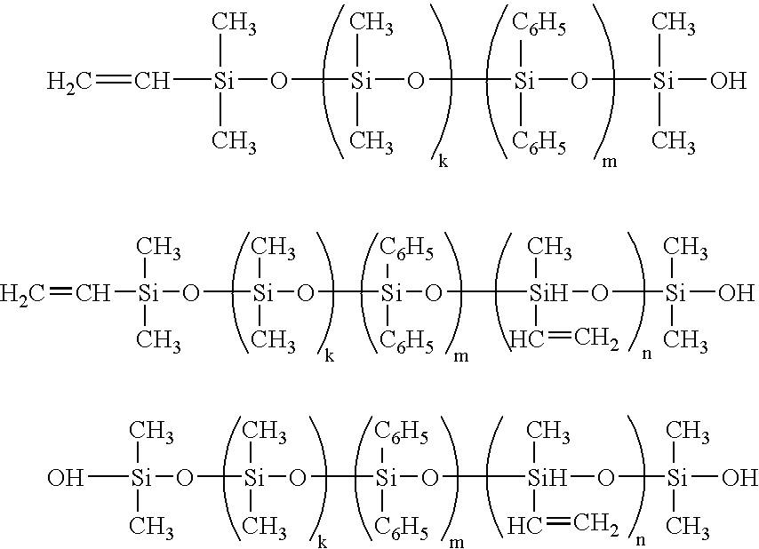
[0071] An epoxy / silicone mixed resin composition was prepared by combining 50 parts of a polysiloxane having formula (i), 30 parts of an organopolysiloxane having a siloxane unit composition (molar ratio) of (PhSiO3 / 2)0.6(MeSiO3 / 2)0.2(ViMeSiO2 / 2)0.2 and containing 8% by weight of silicon atom-bonded hydroxyl groups, 20 parts of a bisphenol A epoxy resin, 5 parts of an organohydrogenpolysiloxane having formula (ii), 0.3 part of an adhesive aid having formula (iii), 0.05 part of an octyl alcohol-modified chloroplatinic acid solution, and 0.1 part of aluminum acetylacetonate and intimately mixing them.

[0072] The composition was heat molded at 150° C. for 4 hours to form a cured sample, which was measured for Shore D hardness according to JIS K-6301. The composition which had been cured at 150° C. for 4 hours was colorless and transparent.

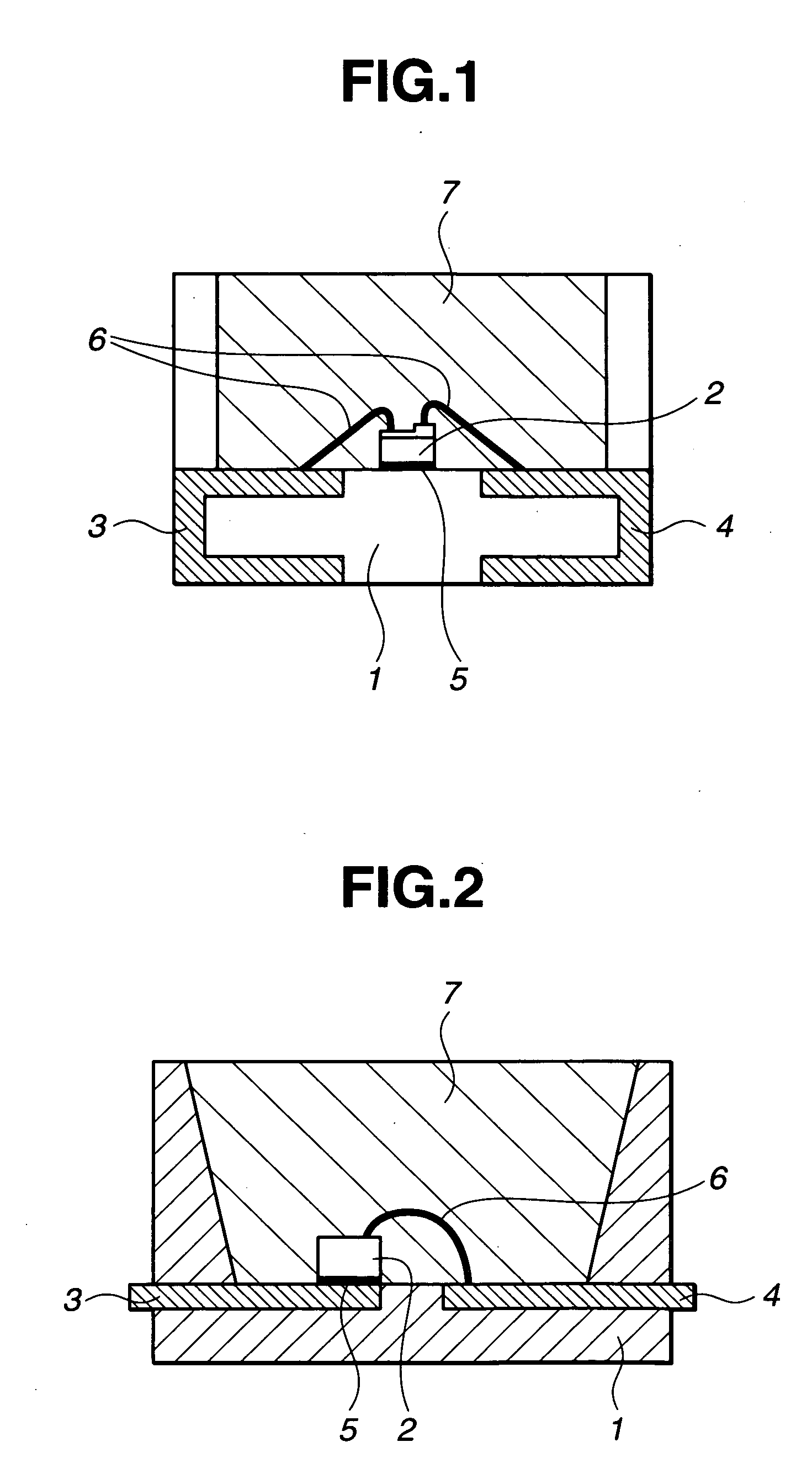
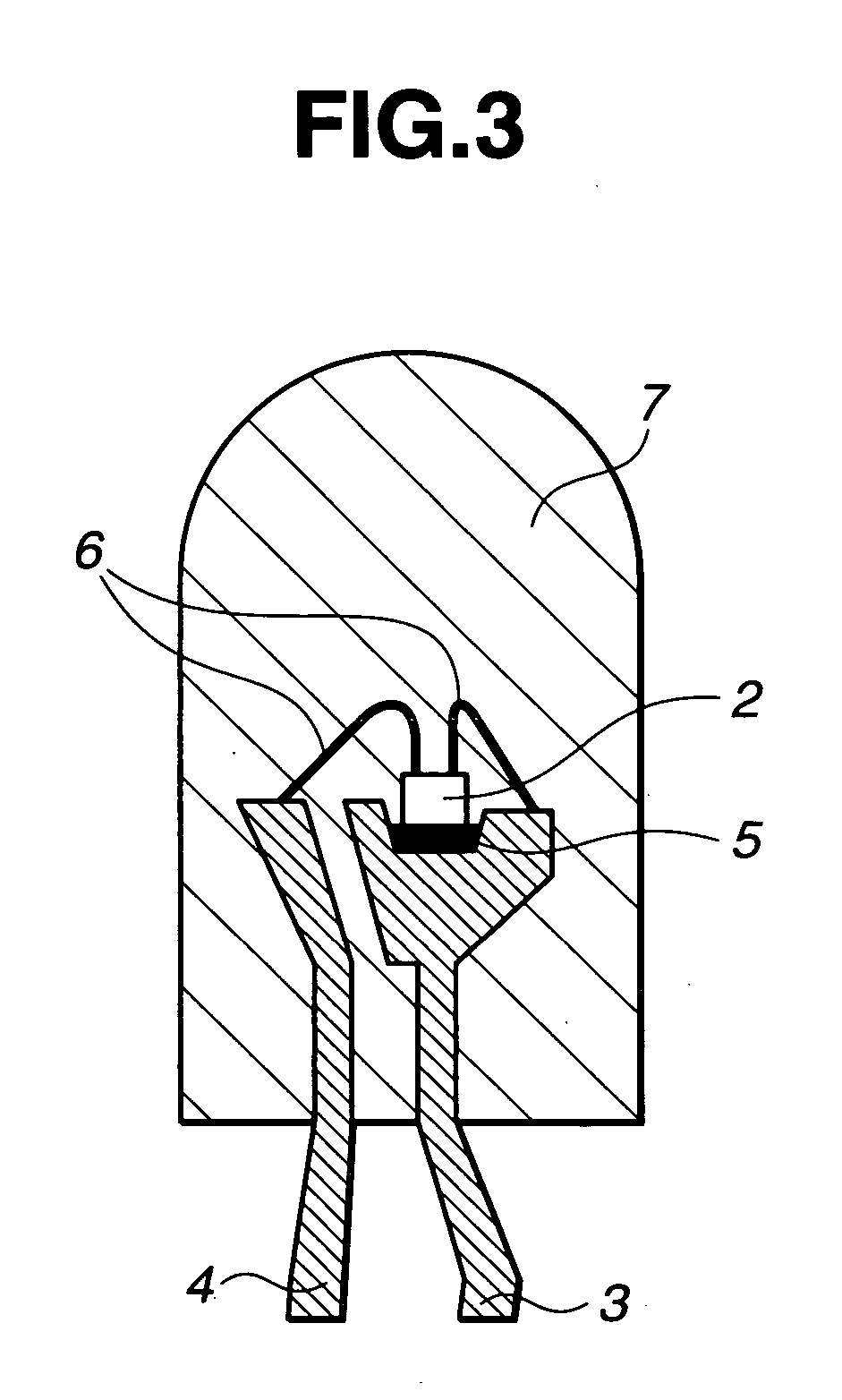
[0073] Using the resin composition, a light-emitting semiconductor device was fabricated as above.

example 2

[0074] An epoxy / silicone mixed resin composition was prepared by combining 80 parts of an organopolysiloxane having a siloxane unit composition (molar ratio) of (PhSiO3 / 2)0.6(MeSiO3 / 2)0.2(ViMeSiO2 / 2)0.2 and containing 8% by weight of silicon atom-bonded hydroxyl groups, 20 parts of a bisphenol A epoxy resin, 5 parts of an organohydrogenpolysiloxane having formula (ii), 0.3 part of an adhesive aid having formula (iii), 0.05 part of an octyl alcohol-modified chloroplatinic acid solution, and 0.1 part of aluminum acetylacetonate and intimately mixing them.

[0075] The composition was heat molded at 150° C. for 4 hours to form a cured sample, which was measured for Shore D hardness according to JIS K-6301. The cured sample was colorless and transparent.

[0076] Using the resin composition, a light-emitting semiconductor device was fabricated as above.


PUM

PropertyMeasurementUnit
viscosity measurementaaaaaaaaaa
molar ratioaaaaaaaaaa

Abstract

An epoxy / silicone mixed resin composition comprising (A′) an organosilicon compound containing at least one aliphatic unsaturated monovalent hydrocarbon group and at least one silicon atom-bonded hydroxyl group, (B) an epoxy resin containing at least one epoxy group, (C) an organohydrogenpolysiloxane, (D) a platinum group metal-based catalyst, and (E) an aluminum-based curing catalyst is used to encapsulate a light-emitting semiconductor member. The light-emitting semiconductor device undergoes little discoloration in a heat test, and has a high emission efficiency, a long life and reduced energy consumption.

Description

CROSS-REFERENCE TO RELATED APPLICATION [0001] This non-provisional application claims priority under 35 U.S.C. §119(a) on Patent Application No. 2003-390482 filed in Japan on Nov. 20, 2003, the entire contents of which are hereby incorporated by reference.TECHNICAL FIELD [0002] This invention relates to epoxy / silicone mixed resin compositions which cure into products free from dust deposition on their surface and having a low elasticity, crack resistance and good adhesion and which are useful as light-emitting semiconductor encapsulants, and light-emitting semiconductor devices encapsulated therewith. BACKGROUND ART [0003] Traditional light-emitting semiconductor devices such as light-emitting diodes (LED) are lamp-type light-emitting semiconductor devices in which a light-emitting semiconductor member is disposed on a lead electrode and encapsulated with a transparent resin to a cannonball shape as shown in FIG. 3. They are recently replaced by the “surface mount” type as a result ...

Claims


Application Information

Patent Timeline
Patent Type & Authority Applications(United States)
IPC IPC(8): C08L63/00C08G59/68C08K3/22C08L83/04C08L83/05C08L83/07H01L23/29H01L33/54H01L33/56H01L33/62
CPCC08G77/045H01L2224/48091C08G77/16C08G77/18C08G77/20C08G77/70C08K3/22C08L63/00C08L83/04H01L23/296H01L33/56C08G77/12H01L2224/32245H01L2224/48247H01L2224/73265H01L2224/45144H01L2224/48257C08L83/00C08L2666/14H01L2924/00014H01L2924/00H01L2924/12044Y10T428/31663Y10T428/31511H01L2924/00012
Inventor KASHIWAGI, TSUTOMUSHIOBARA, TOSHIO
Owner SHIN ETSU CHEM IND CO LTD
Why Eureka
Try Eureka