
Semiconductor device

a technology of semiconductor devices and diodes, which is applied in the direction of semiconductor devices, diodes, electrical apparatus, etc., can solve the problems the formation of the schottky diode is associated with more complexity of manufacturing processes, and the device is more complex, so as to reduce the effect of reducing the area of the device and reducing the complexity of manufacturing processes

Active Publication Date: 2005-06-23
NISSAN MOTOR CO LTD
View PDF4 Cites 25 Cited by
  • Summary
  • Abstract
  • Description
  • Claims
  • Application Information

AI Technical Summary

Problems solved by technology

Accordingly, formation of the Schottky diode has been associated with more complexity of manufacturing processes in comparison with the case of forming only the MOSFET.
As described above, the switching element incorporating the Schottky diode according to the related art has the problems in a reduction of an area of the device, which is directly linked with the manufacturing costs, and in a reduction of the manufacturing processes.

Method used


Image

  • Semiconductor device
  • Semiconductor device
  • Semiconductor device

Examples


first embodiment

[Configuration]

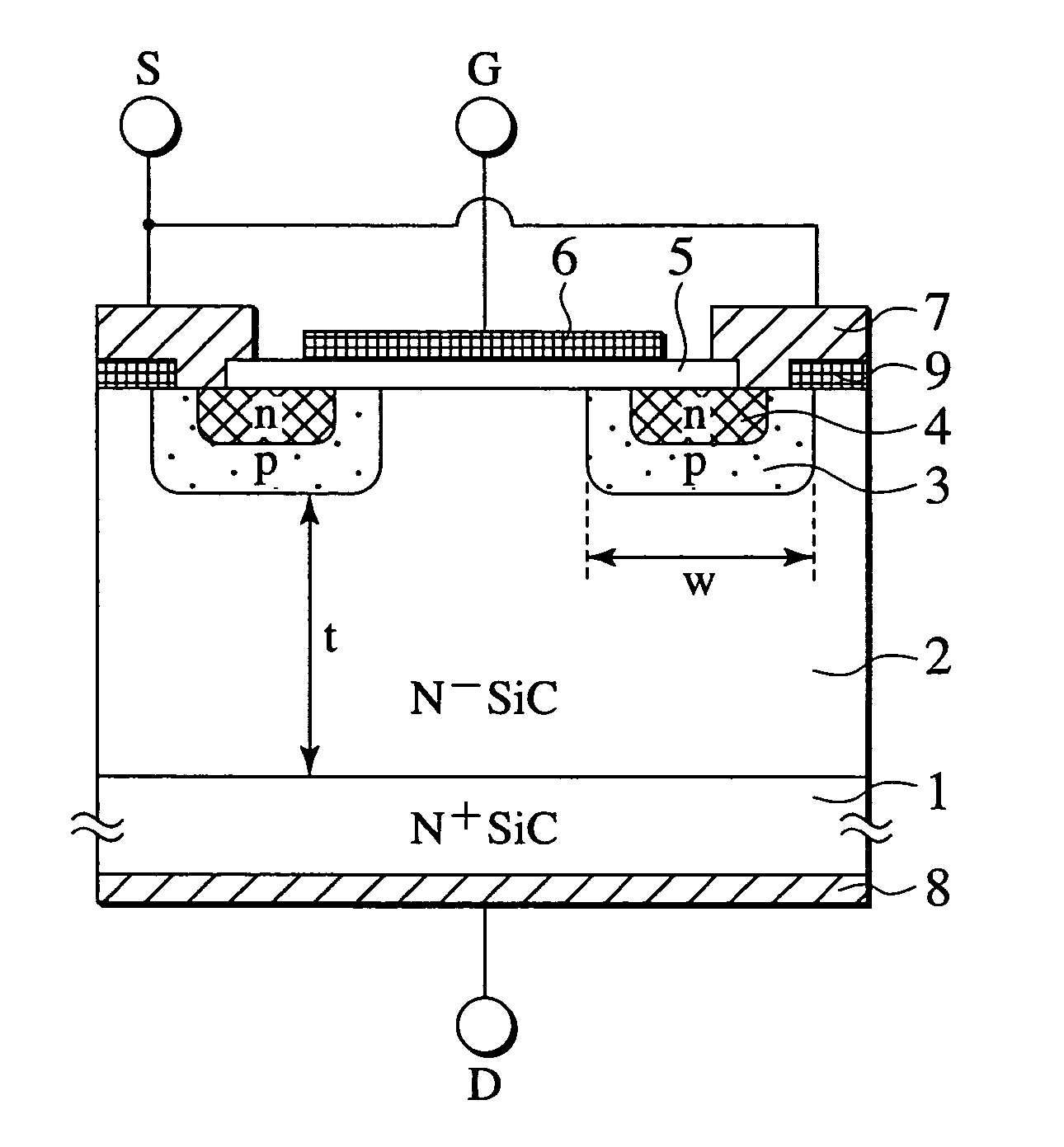
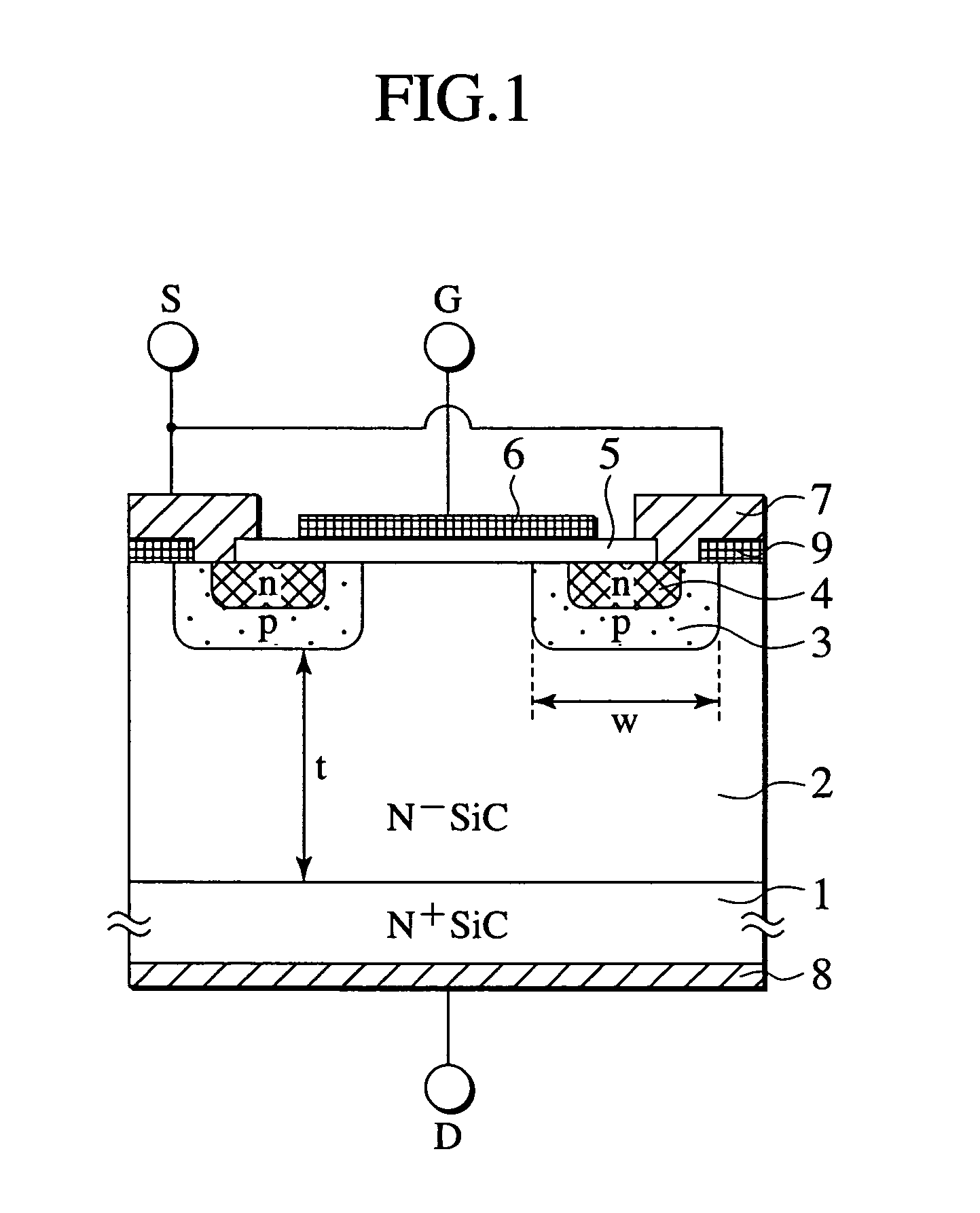
[0028]FIG. 1 is a cross-sectional view showing a semiconductor device according to a first embodiment of the present invention. As shown in FIG. 1, a semiconductor device according to the first embodiment is formed on a semiconductor substrate in which an N−-type drain region 2 is formed on a substrate region 1 made of N+-type silicon carbide of the 4H polytype, for example. A P-type base region 3 is disposed on an upper part of the drain region 2 including a principal surface of the drain region 2, which is opposite to a joint surface between the drain region 2 and the substrate region 1. An N+-type source region 4 is disposed above the base region 3 including the principal surface of the drain region 2. A gate electrode 6 made of N-type polycrystalline silicon, for example, is disposed above the drain region 2, the base region 3, and the source region 4 through an insulating film 5. Further, the base region 3 and the source region 4 are connected to a source electr...

second embodiment

[0058]FIG. 14 is a cross-sectional view corresponding to FIG. 1, which shows a semiconductor device according to a second embodiment of the present invention. In the second embodiment, description of the constituents performing the same operations as those in the semiconductor device shown in FIG. 1 will be omitted. Instead, differences from the semiconductor device shown in FIG. 1 will be described in detail.

[0059] As shown in FIG. 14, the heterojunction semiconductor region 9 is formed deeper than the base region 3. That is to say, a thickness k of the drain region 2 immediately below the heterojunction semiconductor region 9 is smaller than the thickness t of the drain region 2 immediately below the base region 3.

[0060] By forming the deeper heterojunction semiconductor region 9, it is possible to obtain the higher top-up voltage Va as compared to the semiconductor device shown in FIG. 1. FIG. 9 is an example of a calculation result showing a relation between a difference betwe...

third embodiment

[0066]FIG. 17 is a cross-sectional view showing a semiconductor device according to a third embodiment of the present invention. FIG. 17 is the cross-sectional view corresponding to FIG. 1 showing the first embodiment. Meanwhile, FIG. 18 is a side view taken along the A-A′ line in FIG. 17. In the third embodiment, description of the constituents performing the same operations as those in the semiconductor device shown in FIG. 1 will be omitted. Instead, differences from the semiconductor device shown in FIG. 1 will be described in detail.

[0067] As shown in FIG. 17 and FIG. 18, the semiconductor device according to the third embodiment has a trench-type MOSFET structure, in which trenches are formed on the surface layer portion of the drain region 2 and the insulating film 5 and the gate electrode 6 are formed inside each of the trenches. Moreover, the heterojunction semiconductor regions 9 are arranged at given intervals along the gate electrodes 6 so as to be interposed between th...


PUM


Abstract

A semiconductor device includes a heterojunction semiconductor region 9, which forms a heterojunction with a drain region 2. The heterojunction semiconductor region 9 is connected to a source electrode 7, and has a band gap different from a band gap of a semiconductor substrate constituting the drain region 2. It is possible to set the size of an energy barrier against conduction electrons, which is formed between the drain region 2 and the heterojunction semiconductor region 9, into a desired size by changing the conductivity type or the impurity density of the heterojunction semiconductor region 9. This is a characteristic not found in a Schottky junction, in which the size of the energy barrier is inherently determined by a work function of a metal material. It is easy to achieve optimal design of a passive element in response to a withstand voltage system of a MOSFET as a switching element. It is also possible to suppress diffusion potential in a reverse conduction mode and to improve a degree of integration per unit area. As a result, it is possible to reduce the size of elements and to simplify manufacturing processes thereof.

Description

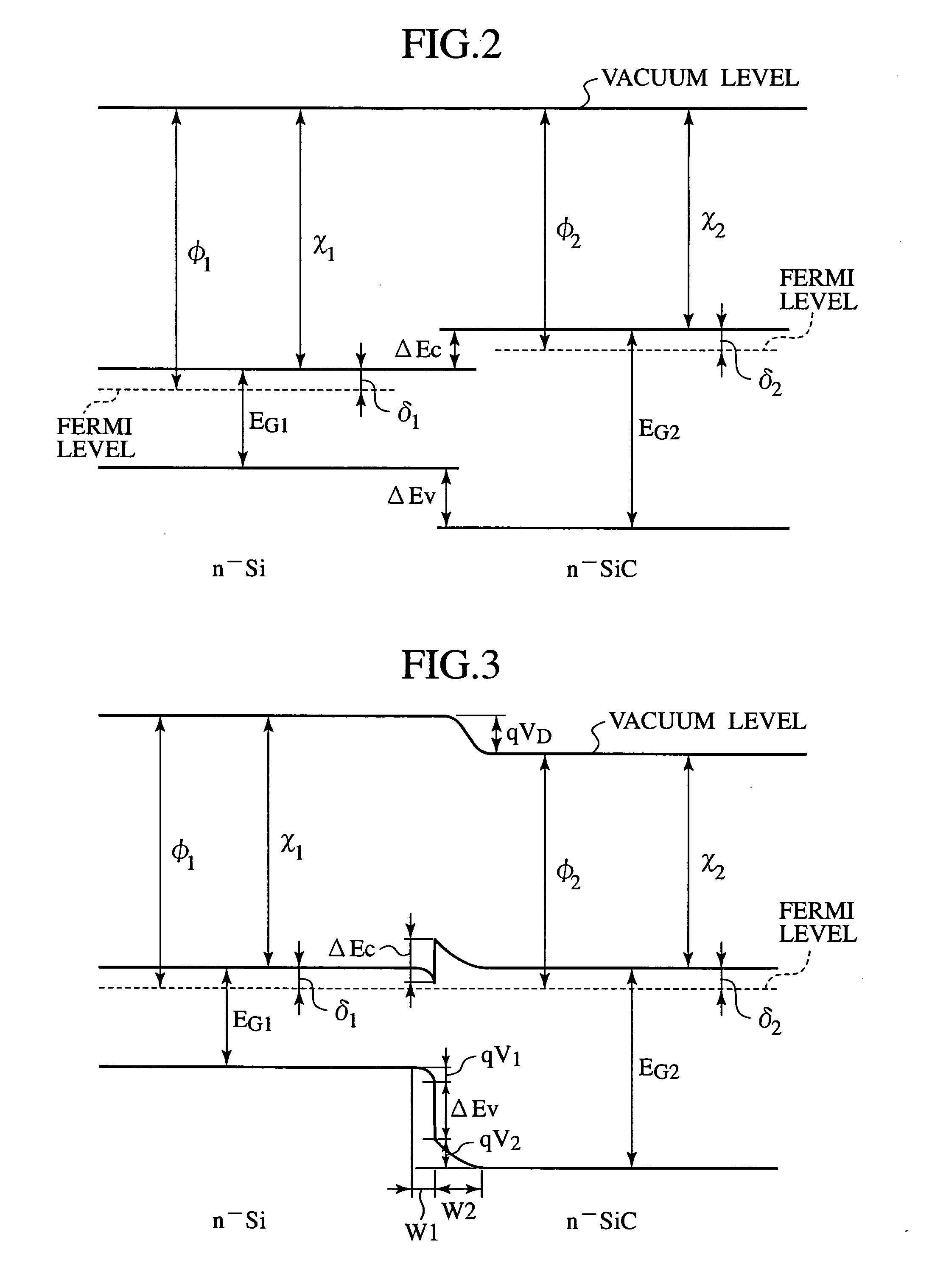
BACKGROUND OF THE INVENTION [0001] The present invention relates to a semiconductor device used as a switching element. As disclosed in Japanese Unexamined Patent Publication No. 2002-299625, a switching element incorporating a Schottky diode in a part of a MOSFET formed on a silicon carbide substrate is known. This switching element is configured to function as a bi-directional conductive element having small switching losses. Specifically, the MOSFET functions as the switching element in the forward conduction mode, while the Schottky diode functions as a majority-carrier passive element in the reverse conduction mode or in so-called the freewheeling action. SUMMARY OF THE INVENTION [0002] However, to operate the Schottky diode as the majority-carrier passive element in the reverse conduction mode, it is necessary to secure a given area for the Schottky diode so as to permit freewheeling of a given current at a potential difference at least equal to or below diffusion potential (3...

Claims


Application Information

Patent Timeline
Patent Type & Authority Applications(United States)
IPC IPC(8): H01L21/28H01L21/336H01L27/04H01L29/12H01L29/15H01L29/24H01L29/267H01L29/47H01L29/78
CPCH01L29/1608H01L29/47H01L29/66068H01L29/7802H01L29/7803H01L29/165H01L29/7813H01L29/7817H01L29/782H01L29/7828H01L29/7806
Inventor HAYASHI, TETSUYAHOSHI, MASAKATSUKANEKO, SAICHIROUTANAKA, HIDEAKI
Owner NISSAN MOTOR CO LTD
Learn More