High-frequency semiconductor device

a semiconductor and high-frequency technology, applied in semiconductor devices, semiconductor/solid-state device details, electrical apparatus, etc., can solve the problems of warping of the mesfet chip and increase the cost, and achieve excellent high-speed performance, small gain reduction, and high power output.

Inactive Publication Date: 2005-06-23
MITSUBISHI ELECTRIC CORP
View PDF3 Cites 51 Cited by
  • Summary
  • Abstract
  • Description
  • Claims
  • Application Information

AI Technical Summary

Benefits of technology

[0020] The present invention has been achieved to solve the conventional disadvantages. It is a first object of the present invention to prov

Problems solved by technology

When the MESFET chip is bonded to the package by die-bonding using the AuSn solder or the like during assembly of the device, warping of the MESFET chip occurs due to a difference in coeffici

Method used


Image

  • High-frequency semiconductor device
  • High-frequency semiconductor device
  • High-frequency semiconductor device

Examples


first embodiment

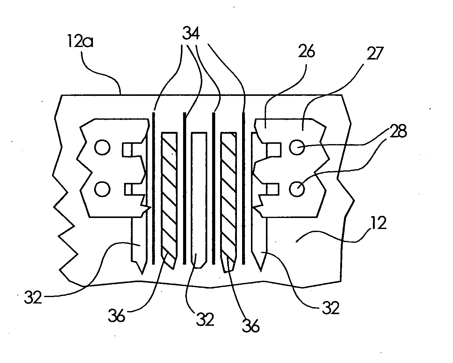
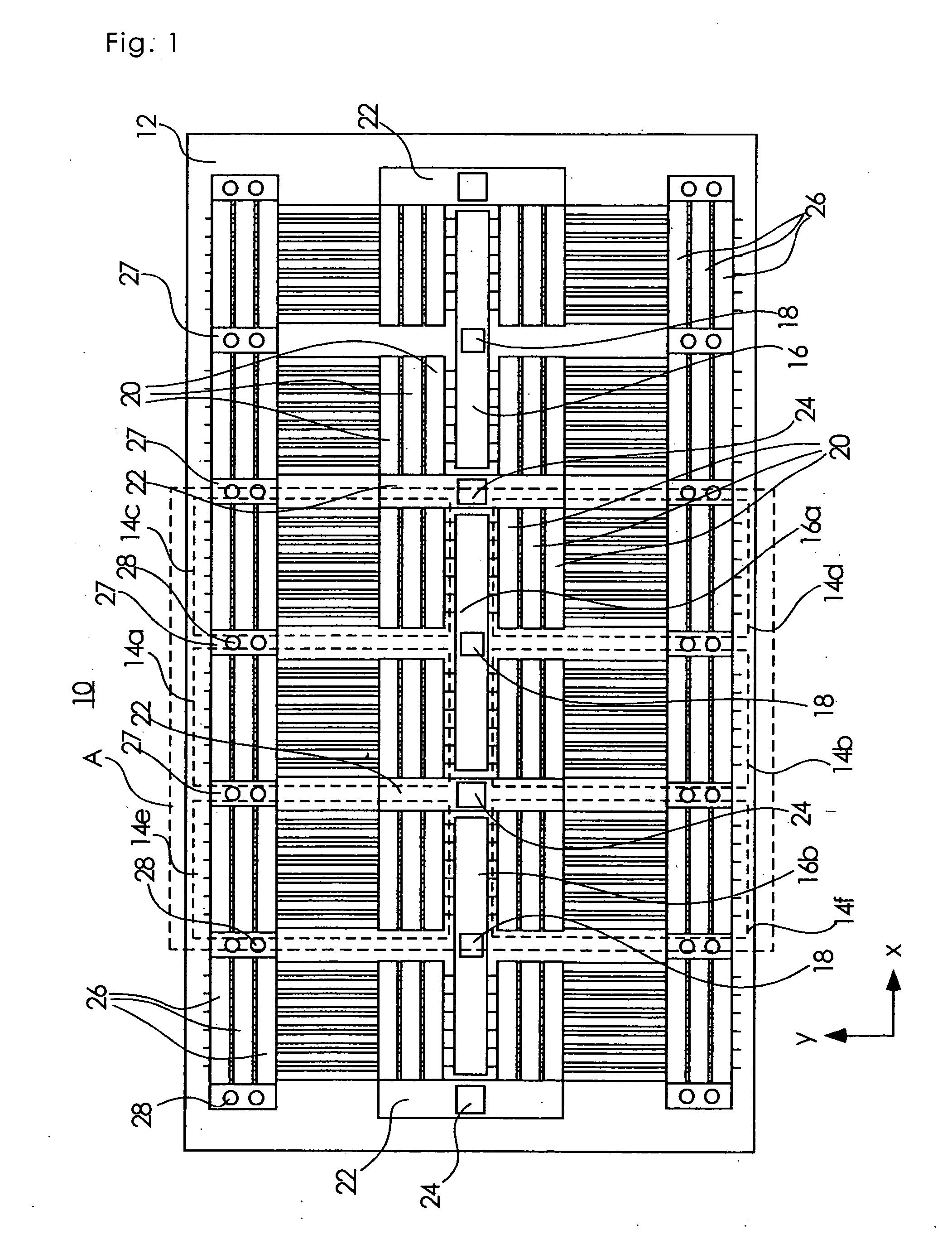
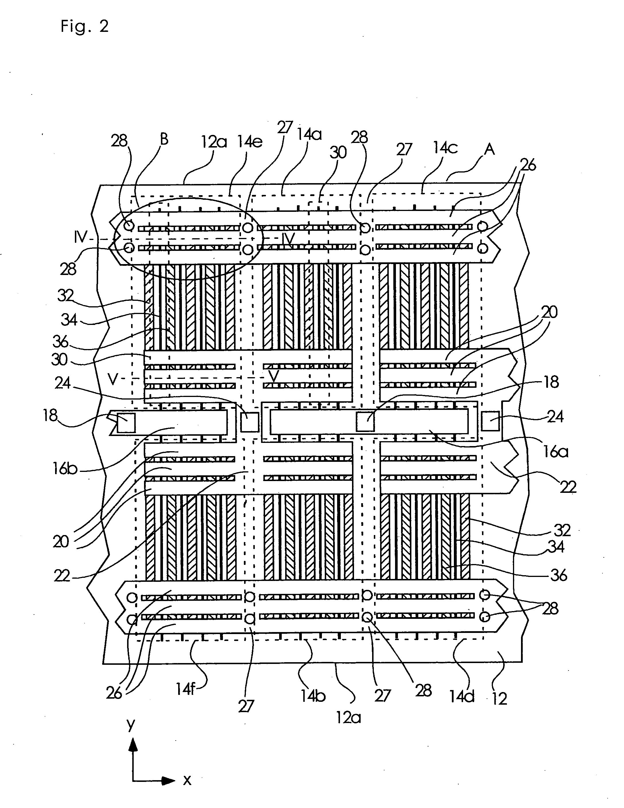
[0034]FIG. 1 is a plan view which depicts a MESFET element according to one embodiment of the present invention. FIG. 2 is a partially enlarged plan view of the MESFET element in a part A shown in FIG. 1. FIG. 3 is a partially broken plan view of the MESFET element in a part B shown in FIG. 2. FIG. 4 is a partially cross-sectional view of the MESFET element taken along a line VI-VI of FIG. 2. FIG. 5 is a partially cross-sectional view of the MESFET element taken along a line V-V of FIG. 2.

[0035] Referring to FIG. 1, the MESFET element 10 is constituted so that a plurality of, e.g., six unit MESFET groups 14a, 14b, 14c, . . . (hereinafter “cells”, which cells are often generically denoted by reference symbol 14), serving as semiconductor element groups each having a plurality of unit MESFET's arranged in parallel in an x-axis direction, are arranged on a semiconductor substrate 12 in the x-axis direction, and are arranged in a plurality of rows, e.g., two rows in a y-axis direction....

second embodiment

[0070]FIG. 7 is a plan view which depicts a MESFET element according to one embodiment of the present invention.

[0071] Referring to FIG. 7, the MESFET element 60 is constituted as follows. In a cell group composed by four cells, e.g., the first cell 14a, the second cell 14b, the third cell 14c, and the fourth cell 14d among which the gate electrode bar 16a is shared, the source pad 27 for connecting the source electrode connection wiring 26 of the first cell 14a to that of the third cell 14c is eliminated. The gate electrode bar 16a is arranged to extend up to outer ends of the first cell 14a and the third cell 14c in the y-axis direction along the sides of the first cell 14a and the third cell 14c between the first cell 14a and the third cell 14c. The gate electrode bar 16, which has an extension, formed into an inverse T shape, in FIG. 7, is provided, and the bonding pad 18 is formed on an outer end of the extension.

[0072] Furthermore, in a cell group composed by four cells, e.g...


PUM


Abstract

A high-frequency semiconductor device includes: a first cell which includes of gate electrodes on a surface of an epitaxial layer of a substrate, drain electrodes and source electrodes alternately located relative to the gate electrodes, a source electrode connection wiring striding over the gate electrodes and the drain electrodes and connecting the source electrodes, and a drain electrode connection wiring striding over the gate electrodes and the source electrodes and connecting the drain electrodes; a second cell which has the same configurations as the first cell, is located in an extended direction of each of the gate electrodes of the first cell, and has the drain electrode connection wiring proximate to the drain electrode connection wiring of the first cell; and a gate electrode bar located between the drain electrode connection wirings of the first and second cells, and to which the gate electrodes of the first and second cells are connected.

Description

BACKGROUND OF THE INVENTION [0001] 1. Field of the Invention [0002] The present invention relates to a high-frequency semiconductor device. More specifically, the present invention relates to a high-frequency semiconductor device for use in a communication apparatus such as a transmitter-receiver for satellite communication or mobile communication. [0003] 2. Description of the Related Art [0004] Following a rapid increase in communication demand, a capacity of a communication system has been intended to be increased. To do so, it is necessary to improve a high speed performance, reduce a size, improve efficiency, cut down a cost of a communication apparatus. [0005] For a microwave device used in the communication apparatus such as a transmitter / receiver for satellite communication or mobile communication which uses high frequencies, metal semiconductor field effect transistors (MESFET's), for example, are employed as transistors having good high frequency characteristics. [0006] If ...

Claims


Application Information

Patent Timeline
IPC IPC(8): H01L21/338H01L21/8234H01L29/41H01L23/482H01L29/06H01L29/812
CPCH01L21/823475H01L23/4821H01L23/4824H01L29/0692H01L29/812H01L2924/0002H01L2924/3011H01L2924/00
Inventor KUNII, TETSUOKAMO, YOSHITAKA
Owner MITSUBISHI ELECTRIC CORP
Why Eureka
Try Eureka