Semiconductor device and fabrication method of a semiconductor device

a technology of semiconductor devices and semiconductor devices, which is applied in the direction of semiconductor devices, capacitors, electrical devices, etc., can solve the problems of severe degradation, degraded capacitor performance, and difficulty in forming a capacitor free from leakage between the upper electrode and the lower electrode with reliability, so as to achieve the effect of simplifying the process

Inactive Publication Date: 2005-06-23
FUJITSU SEMICON LTD
View PDF2 Cites 6 Cited by
  • Summary
  • Abstract
  • Description
  • Claims
  • Application Information

AI Technical Summary

Benefits of technology

[0013] Another and more specific object of the present invention is to provide a semiconductor device having a reliable ferroelectric capacitor wherein efficiency of surface area utilization is improved and capacitor degradation and leakage are eliminated.
[0037] Preferably, the forming step of the upper electrode includes the step of patterning the upper electrode in the form of the plate line. With this, the step for forming the plate line for connecting the isolated upper electrodes is eliminated, and the process can be simplified.

Problems solved by technology

On the other hand, even when such high temperature etching technology is used, it is difficult to form a capacitor free from leakage between the upper electrode and the lower electrode with reliability.
Thereby, the reducing reaction associated with the penetrated hydrogen molecules causes the problem that the capacitor performance is degraded.
Thereby, there occurs loss of lead, and severe degradation may be caused.
When such degradation of capacitor is caused, there occurs a reduction of effective area in the final capacitor, contrary to the effort of improving the surface area utilization efficiency by conducting one-step etching with near vertical angle.

Method used


Image

  • Semiconductor device and fabrication method of a semiconductor device
  • Semiconductor device and fabrication method of a semiconductor device
  • Semiconductor device and fabrication method of a semiconductor device

Examples


first embodiment

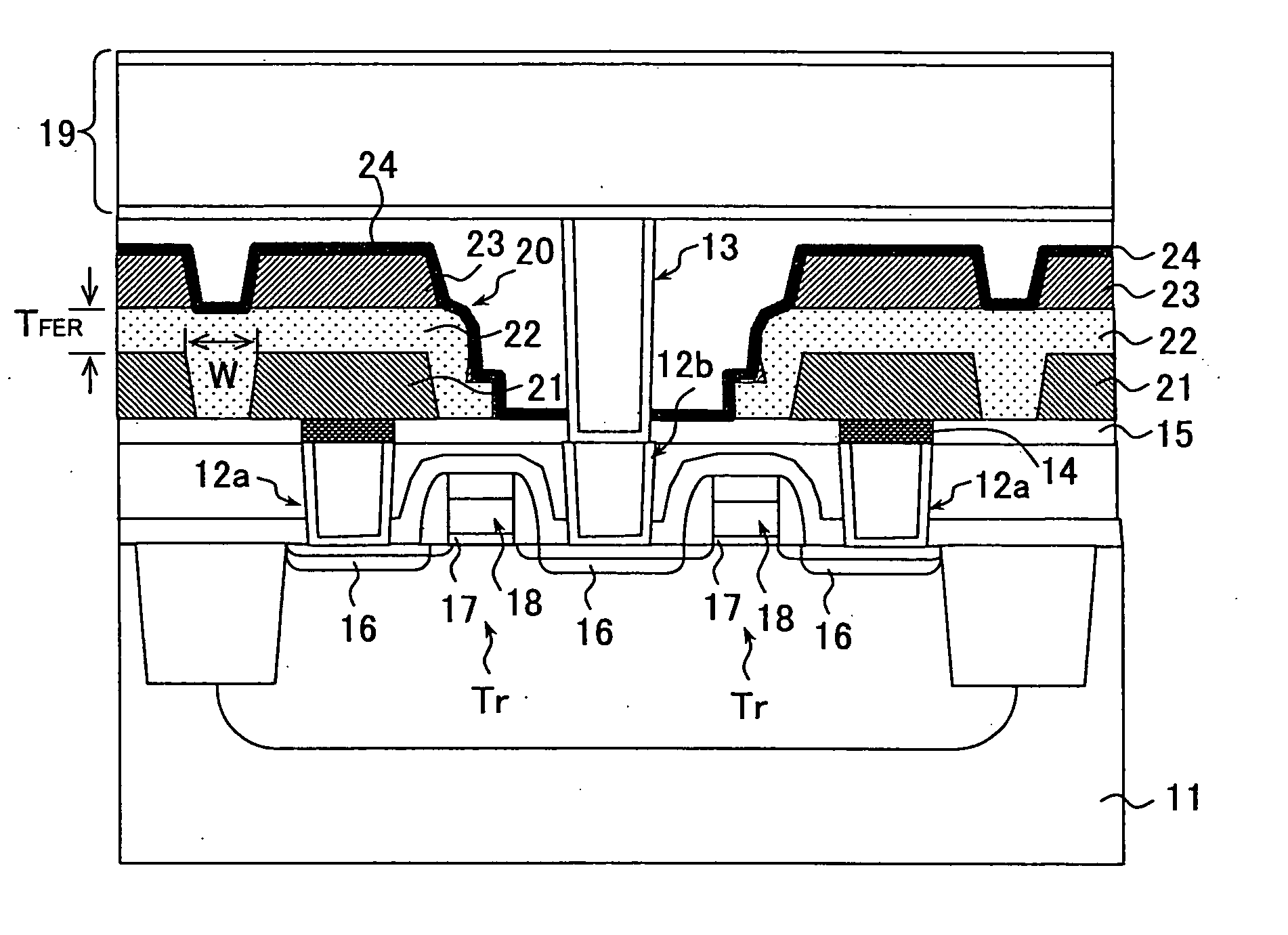
[0066] In the first embodiment, the upper electrode 23 is not isolated but has a shape of the plate line pattern. Because the upper electrode 23 functions as the plate line as it is, there is no need of providing additional interconnection wiring.

[0067] Thus, with the semiconductor device of the first embodiment, the ferroelectric film 22 of the ferroelectric capacitor 20 covers the lower electrode 21 continuously except for the region surrounding the bit line contact 13, and unwanted exposure of the sidewall of the ferroelectric film 22 is minimized. As a result, degradation of the ferroelectric film such as the one caused by process degradation including loss of lead, is successfully minimized even after various processes are conducted in the reducing ambient. Thereby, the reliability of operation is improved.

[0068] Further, by setting the interval between adjacent lower electrodes 21 and the thickness of the ferroelectric film 22 so as to satisfy the condition (1) except for the...

second embodiment

[0105] Next, the present invention will be described.

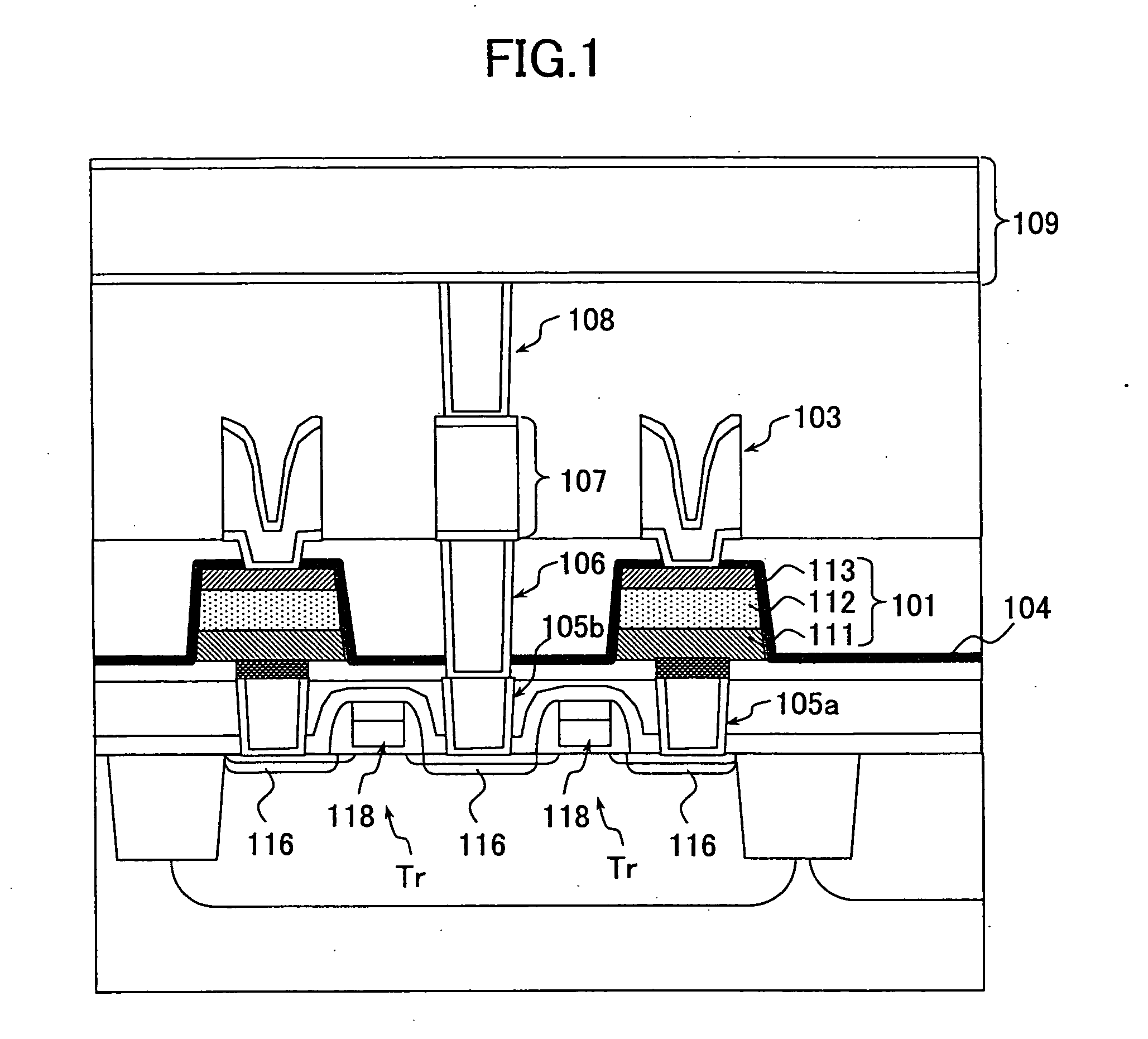
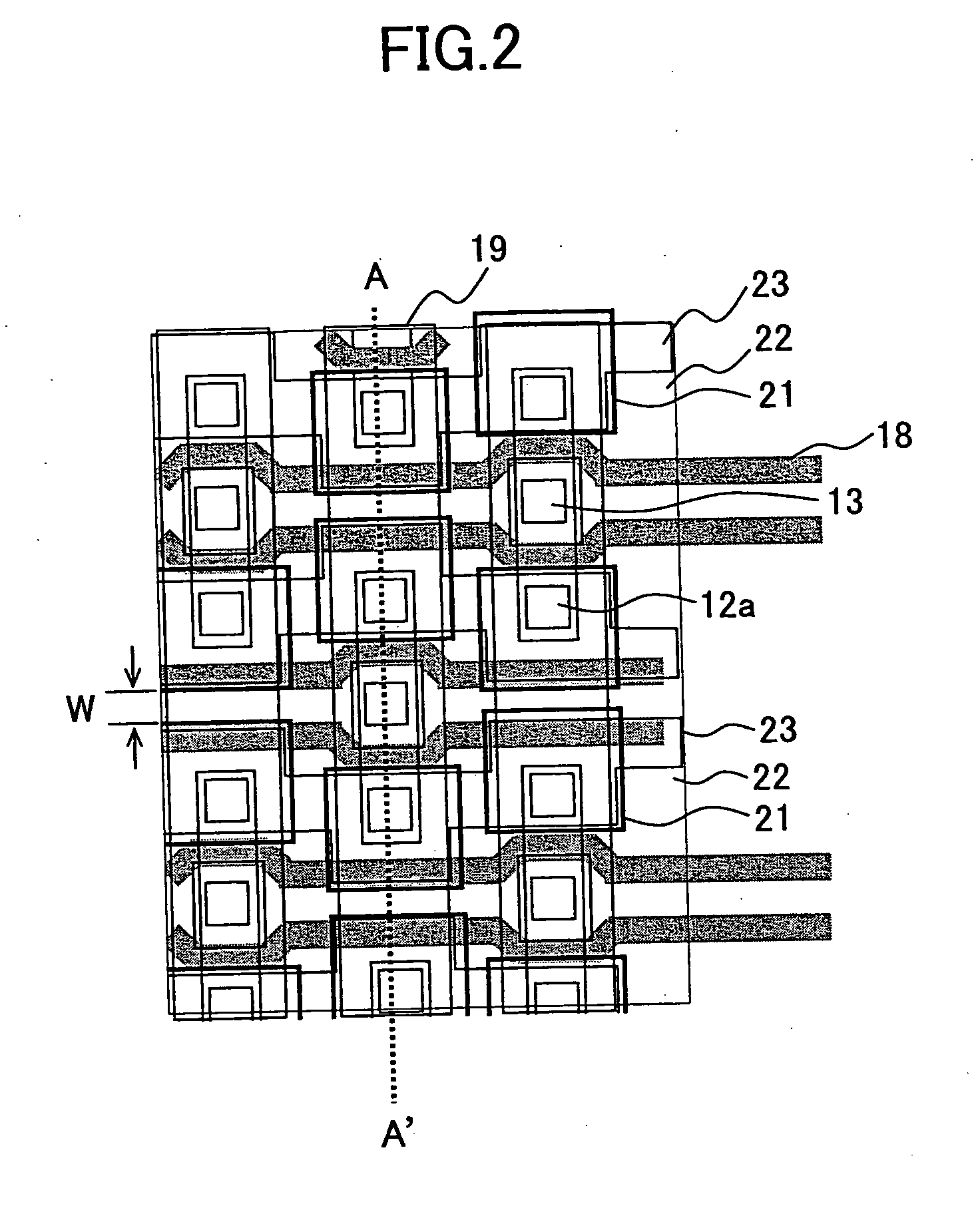
[0106]FIGS. 18 and 19 are diagrams showing the semiconductor device according to a second embodiment of the present invention. FIG. 18 is a top plan view of the semiconductor device of the second embodiment, while FIG. 19 is a cross-sectional view taken along an A-A′ line of FIG. 18.

[0107] In the first embodiment, the upper electrode 23 is patterned according to the shape of the plate line and the upper electrode 23 has been used also as the plate line. In the second embodiment, on the other hand, the upper electrode 53 is formed to have a shape corresponding to the lower electrode 21, and a plate line 63 is provided separately. Thus, the ferroelectric capacitor 50 is formed of the lower electrode 21, a part of the ferroelectric film 22 covering the lower electrode continuously, the part corresponding to the lower electrode, and an isolated upper electrode 43 opposing the lower electrode 21 across the ferroelectric film.

[0108] I...

third embodiment

[0116] Next, the present invention will be described.

[0117]FIGS. 22 and 23 are diagrams showing the semiconductor device according to a third embodiment of the present invention, wherein FIG. 22 is a top plan view of the semiconductor device of the third embodiment, while FIG. 23 is a cross-sectional view of FIG. 22 taken along the line A-A′ of FIG. 22. In the drawings, those parts corresponding to the parts explained previously are designated by the same reference numerals and the description thereof will be omitted.

[0118] As shown in FIGS. 22 and 23, the semiconductor device according to the third embodiment includes the transistors Tr formed on the semiconductor substrate, the plural lower electrodes 21 each connected to one of the diffusion regions 16 of the corresponding transistor Tr, a ferroelectric film 82 covering the surface 21-1 and the sidewall surface 21-1 of the plural electrodes 21 continuously except for the predetermined regions, and the upper electrode 23 provided...


PUM


Abstract

In a conventional semiconductor device provided with a conventional stacked type ferroelectric capacitor, there has been caused a problem of capacitor degradation by leakage between an upper electrode and a lower electrode via an etching reside, when the efficiency of utilization of a surface area is increased by decreasing the interval between the capacitors in the in-plane direction of the substrate, as a result of the one-step annealing of the laminated from of lower electrode film / ferroelectric film / upper electrode film. The present invention prevents leakage caused by short circuit between the lower electrode and the upper electrode, by forming plural lower electrodes, forming a ferroelectric film so as to cover the surface and sidewall surface of the lower electrodes and forming an upper electrode on the ferroelectric film so as to oppose with the lower electrodes. Further, as a result of forming the ferroelectric film so as to cover the lower electrodes continuously and by setting the interval between the lower electrodes and the thickness of the ferroelectric film to satisfy a predetermined relationship, the surface of the ferroelectric film is planarized and exposure of the sidewall is suppressed. Thereby, degradation of the capacitor is prevented.

Description

CROSS-REFERENCE TO RELATED APPLICATIONS [0001] The present invention is a continuation application filed under 35 U.S.C. 111(a) claiming benefit under 35 U.S.C. 120 and 365(c) of PCT application PCT / JP2003 / 014656 filed on Nov. 18, 2003, which in turn is based on Japanese priority application 2002-333500 filed on Nov. 18, 2002, the entire contents of which are incorporated herein as reference.BACKGROUND OF THE INVENTION [0002] The present invention relates to semiconductor devices and the fabrication method thereof, and particularly a semiconductor device having a ferroelectric capacitor and the fabrication method thereof. [0003] With the demand of higher integration density, FeRAM devices constituting a ferroelectric memory are also subjected to the demand of further miniaturization. In relation to this, efforts are being made on the development of the FeRAM device having a stacked structure in place of the planar structure (Reference should be made to Patent Reference 1 or 2, for e...

Claims


Application Information

Patent Timeline
Patent Type & Authority Applications(United States)
IPC IPC(8): H01L21/00H01L21/02H01L21/768H01L21/8246H01L27/115H01L29/76
CPCH01L21/76829H01L21/7687H01L27/11502H01L28/75H01L28/55H01L28/57H01L28/65H01L27/11507H10B53/30H10B53/00
Inventor OKITA, YOICHI
Owner FUJITSU SEMICON LTD
Why Eureka
Try Eureka