Transistor design and layout for performance improvement with strain

a technology of strain and strain, applied in the direction of semiconductor devices, basic electric elements, electrical apparatus, etc., can solve the problems of short channel effect, deformation of mobility, negative impact on channel mobility, etc., to facilitate electron and hole mobility, facilitate performance and fabrication of semiconductor devices, and improve electron mobility

Active Publication Date: 2005-06-30
TEXAS INSTR INC
View PDF6 Cites 43 Cited by
  • Summary
  • Abstract
  • Description
  • Claims
  • Application Information

AI Technical Summary

Benefits of technology

[0008] The present invention includes structure and process improvements that facilitate performance and fabrication of semiconductor devices. The present invention provides for a semiconductor device and layout that can improve electron mobility for N type (NMOS devices) and hole mobility for P type (PMOS devices) by aligning the devices channel regions, respectively, along suitable crystallographic orientation axes of a semiconductor substrate. Furthermore, the present invention further facilitates the electron and hole mobility for the N type and P type devices, respectively, by selectively applying strain to the channel regions.
[0009] The semiconductor device of the present invention is fabricated on a semiconductor substrate that has a first and second crystallographic orientation axes (e.g., <110>, <100>). Source to drain channel regions for P type devices are aligned along the first crystallographic orientation axis. Source to drain channel regions for N type devices are rotated from the channel regions of the P type devices by an offset angle so that the source to drain channel regions for the N type devices are aligned with the second crystallographic orientation axis. Subsequently, a uniaxial or biaxial tensile stress is applied to the source to drain channel regions of the N type devices and a uniaxial or biaxial compressive stress is applied to the source to drain channel regions of the P type devices. In the above manner, carrier mobility is enhanced for both NMOS and PMOS devices, concurrently, on the same die.

Problems solved by technology

Such shrinkage can negatively impact channel mobility and lead to problems such as short channel effects.
For some devices, types of strain improve mobility whereas other degrade mobility.
A problem with applying strain to a semiconductor device is that the strain can improve performance for one type of device (e.g., PMOS) while at the same time degrading performance of another type of device (e.g., NMOS).
As a result, tradeoffs are often made in conventional devices for performance of one type versus another.

Method used


Image

  • Transistor design and layout for performance improvement with strain
  • Transistor design and layout for performance improvement with strain
  • Transistor design and layout for performance improvement with strain

Examples


Embodiment Construction

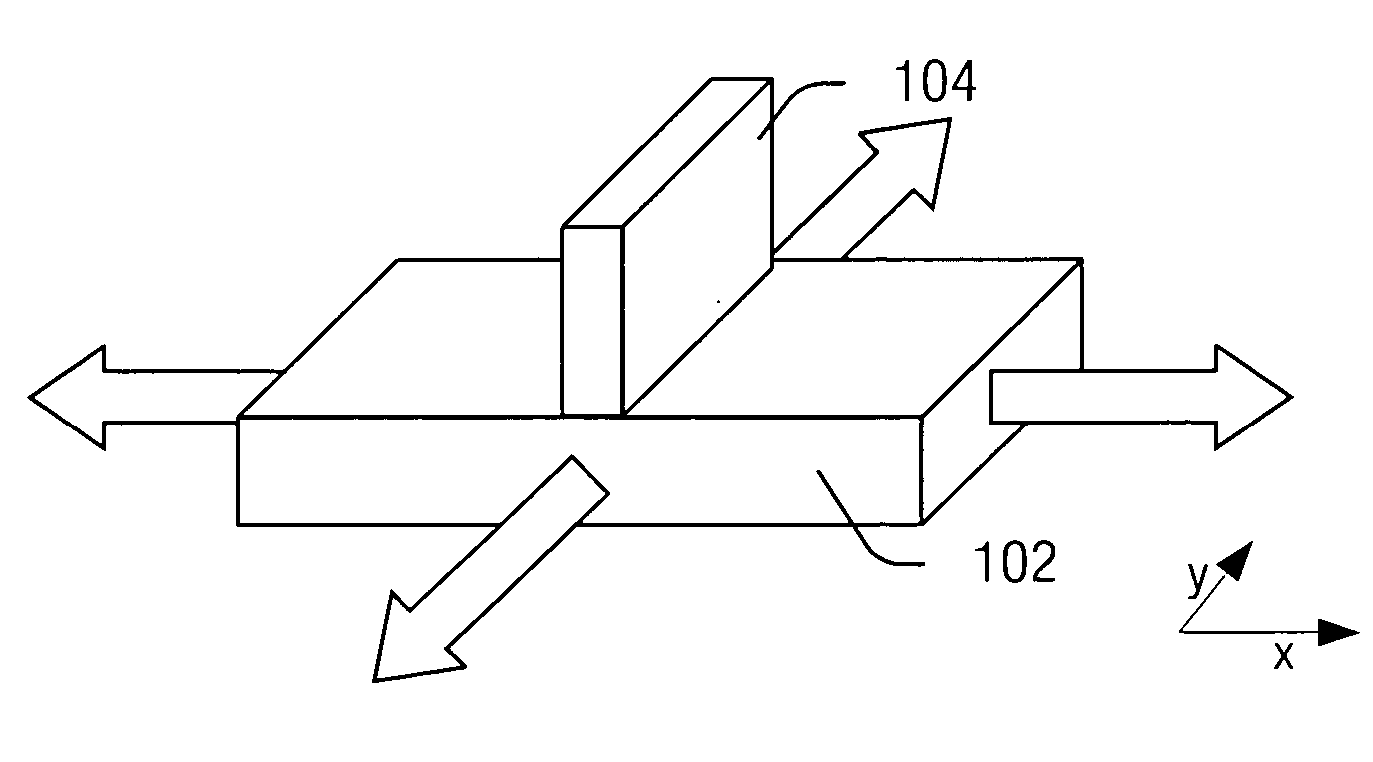
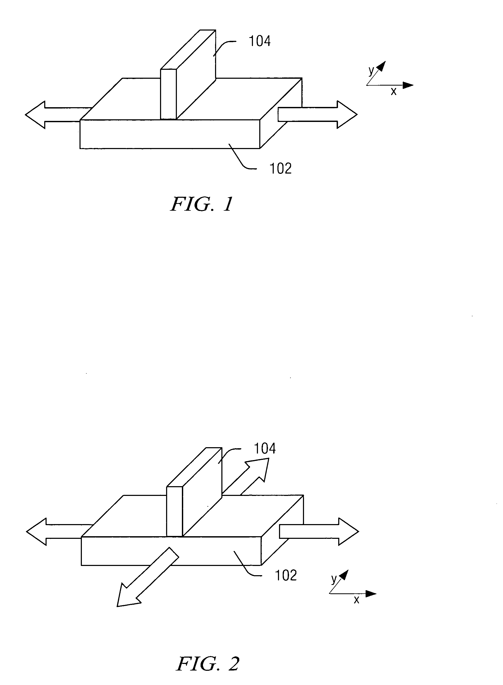
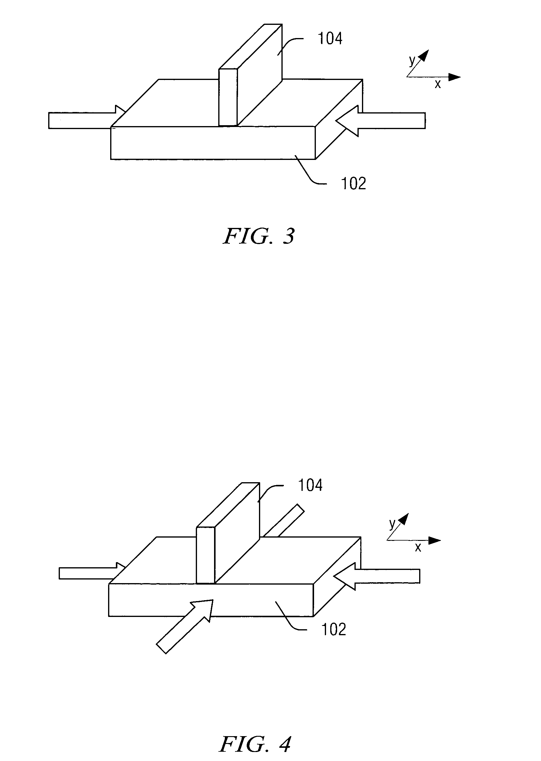
[0021] The present invention will now be described with respect to the accompanying drawings in which like numbered elements represent like parts. The figures provided herewith and the accompanying description of the figures are merely provided for illustrative purposes. One of ordinary skill in the art should realize, based on the instant description, other implementations and methods for fabricating the devices and structures illustrated in the figures and in the following description.

[0022] There is an ongoing need to scale components and features of semiconductor devices. Scaling can reduce costs of fabrication by fitting more components on a single device and can improve performance by shortening paths of operation. As the dimensions on components of a semiconductor device (e.g., chip) continue to be reduced, a key component is a transistor, and a key dimension of the transistor is the gate length. For example, an increase in operation from a 400 Mhz semiconductor device to a ...


PUM


Abstract

The present invention facilitates semiconductor device fabrication and performance by providing a semiconductor device that can improve channel mobility for both N type and P type transistor devices. The semiconductor device of the present invention is fabricated on a semiconductor substrate 802 that has a first and second crystallographic orientation axes (e.g., <110>, <100>) 804 and 806. Source to drain channel regions for P type devices are formed 904 and aligned along the first crystallographic orientation axis. Source to drain channel regions for N type devices are formed 906 rotated from the channel regions of the P type devices by an offset angle so that the source to drain channel regions for the N type devices are aligned with the second crystallographic orientation axis. Subsequently, a uniaxial or biaxial tensile stress 908 is applied to the source to drain channel regions of the N type devices and a uniaxial or biaxial compressive stress 910 is applied to the source to drain channel regions of the P type devices.

Description

RELATED APPLICATIONS [0001] This application claims the priority of U.S. Provisional Application Ser. No. 60 / 533,774, filed Dec. 30, 2003, entitled TRANSISTOR DESIGN AND LAYOUT FOR PERFORMANCE IMPROVEMENT WITH STRAIN.FIELD OF THE INVENTION [0002] The present invention relates generally to the field of semiconductor devices, and more particularly, to systems and methods that facilitate scaling and performance by improving channel mobility for N type and P type transistor devices. BACKGROUND OF THE INVENTION [0003] There exists a continuing need to improve semiconductor device performance and further scale semiconductor devices. These needs can be met by improvements in two broad categories; process and structure. Process improvements are those that allow the fabrication of devices and circuits with smaller dimensions in ever higher density, quantity and reliability. The structure improvements include new device designs that allow greater circuit performance, control and reliability. ...

Claims


Application Information

Patent Timeline
Patent Type & Authority Applications(United States)
IPC IPC(8): H01L21/336H01L29/04H01L29/417H01L29/78
CPCH01L29/045H01L29/41758H01L29/7842H01L29/78H01L29/66477
Inventor ROST, TIMOTHY A.
Owner TEXAS INSTR INC
Why Eureka
Try Eureka