Method for forming copper wiring of semiconductor device

Inactive Publication Date: 2005-06-30
DONGBU ELECTRONICS CO LTD
View PDF12 Cites 22 Cited by
  • Summary
  • Abstract
  • Description
  • Claims
  • Application Information

AI Technical Summary

Benefits of technology

[0010] The present invention has been made in an effort to solve the above problems, and it is an object of the present invention to provide a method for forming a co

Problems solved by technology

However, it becomes difficult to form fine metal wiring patterns due to the reduction of the critical dimension of the metal wiring as the semiconductor devices become

Method used


Image

  • Method for forming copper wiring of semiconductor device
  • Method for forming copper wiring of semiconductor device
  • Method for forming copper wiring of semiconductor device

Examples


Embodiment Construction

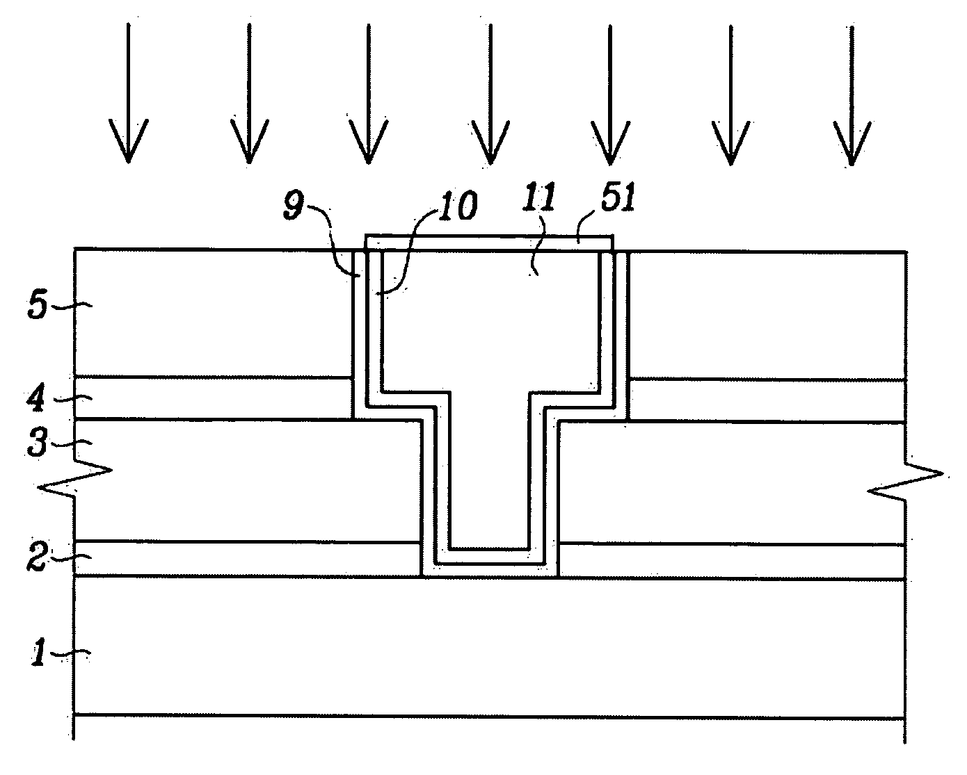
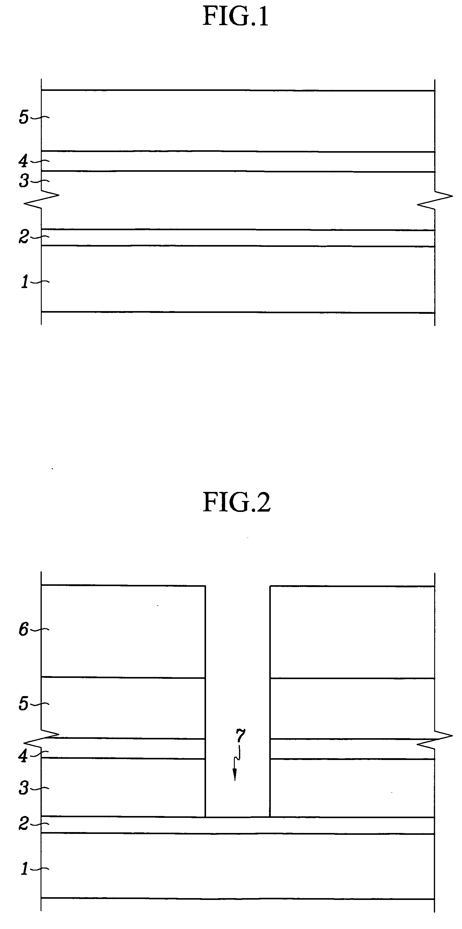
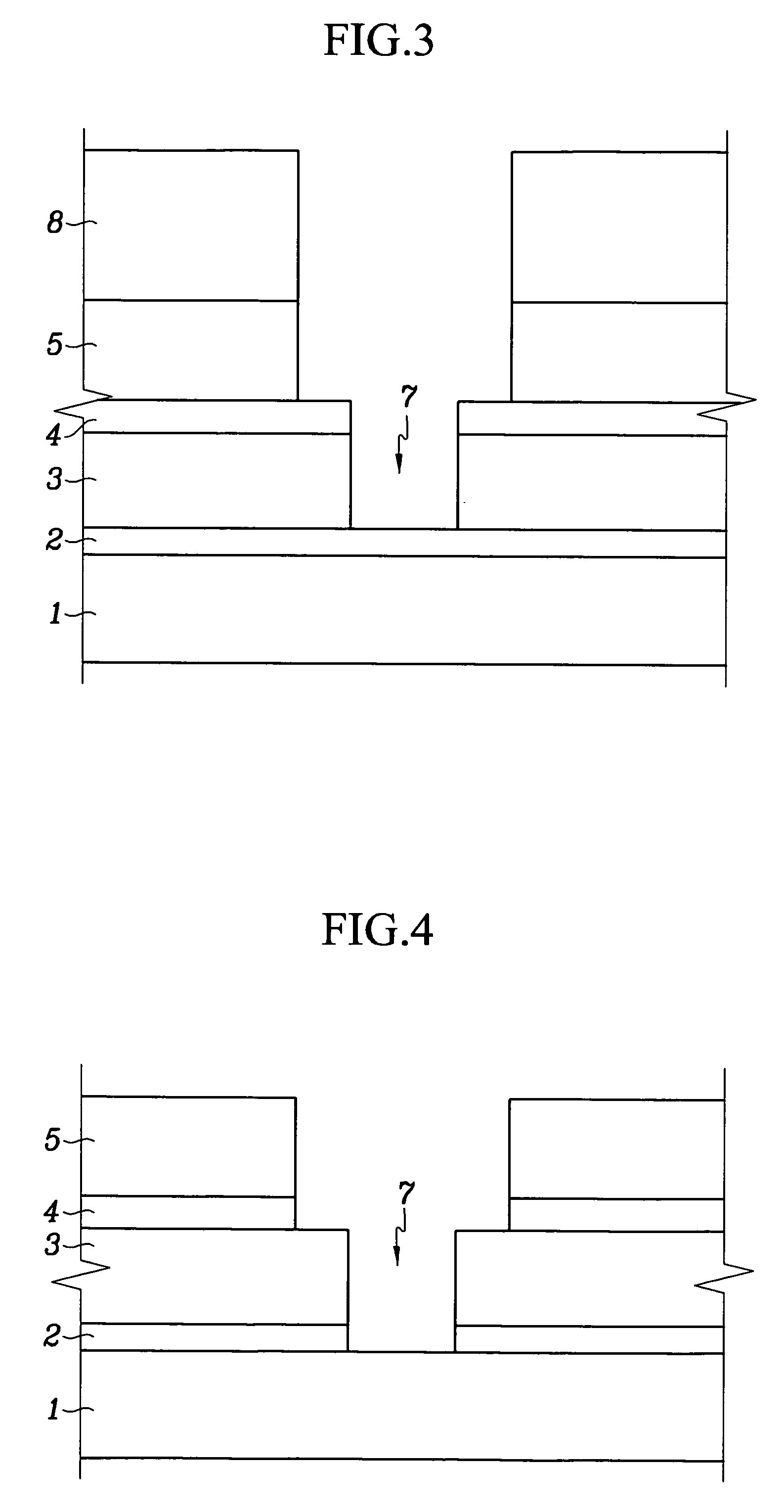
[0017] With reference to the accompanying drawings, the present invention will be described in order for those skilled in the art to be able to implement the same. However, the invention is not limited to the embodiments to be described hereinafter, but, to the contrary, the invention is intended to cover various modifications and equivalent arrangements included within the sprit and scope of the appended claims.

[0018] To clarify multiple layers and regions, the thicknesses of the layers are enlarged in the drawings. Wherever possible, the same reference numbers will be used throughout the drawing(s) to refer to the same or like parts or structures. When it is said any part or structure such as a layer, film, area, or plate is positioned on another part or structure, it means the part is directly on the other part or above the other part with at least one intermediate part or structure therebetween. Any part or structure that is positioned directly on another part or structure mean...


PUM


Abstract

The method for forming the copper wiring of the semiconductor device includes the steps of forming a first copper wiring on a semiconductor substrate having a predetermined low structure, implanting magnesium ion on the first copper wiring, forming a magnesium oxide layer on the first copper wiring by thermal treating the first copper wiring, and forming a second copper wiring on the magnesium oxide layer.

Description

BACKGROUND OF THE INVENTION [0001] (a) Field of the Invention [0002] The present disclosures to a method for forming metal wiring and, in particular, to a method for forming the metal wiring of a semiconductor device using a dual damascene process. [0003] (b) Description of the Related Art [0004] Typically, the metal wiring of a semiconductor device is formed out of thin metal films such as aluminum, aluminum alloy, or copper on a semiconductor substrate so as to electrically connect the circuits formed in the semiconductor substrate. Such metal wiring, which connects the device electrodes and pads isolated by a dielectric layer such as an oxide layer, is generally formed in the order of selectively etching the dielectric layer so as to form contact holes and filling the contact holes with plugs using barrier metal and tungsten, forming a metal thin film thereon, and patterning the metal thin film so as to contact the device electrodes and pads to each other. [0005] In order to patt...

Claims


Application Information

Patent Timeline
IPC IPC(8): H01L21/28H01L21/4763H01L21/768H01L23/48H01L23/52H01L23/532
CPCH01L21/76801H01L21/76807H01L21/76834H01L21/76883H01L21/76886H01L21/76888H01L2924/0002H01L23/53238H01L23/53295H01L2924/00H01L21/28
Inventor JUNG, BYUNG-HYUN
Owner DONGBU ELECTRONICS CO LTD
Why Eureka
Try Eureka