Organic electroluminescent device
a technology of electroluminescent devices and electroluminescent tubes, which is applied in the direction of discharge tube luminescnet screens, other domestic articles, natural mineral layered products, etc., can solve the problem of slow emission response and achieve the effect of high luminance and high durability
- Summary
- Abstract
- Description
- Claims
- Application Information
AI Technical Summary
Benefits of technology
Problems solved by technology
Method used
Image
Examples
example 1
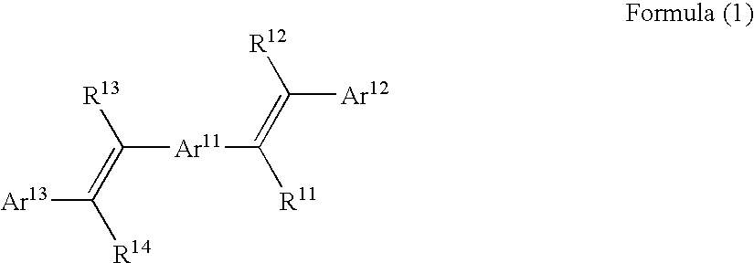
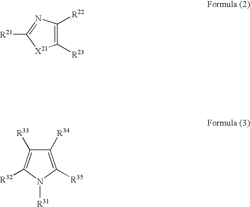
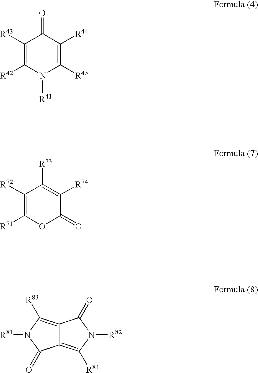
[0139] A washed ITO substrate was placed in a vapor-deposition apparatus, and TPD (N,N′-diphenyl-N,N′-di(m-natholyl)-benzidine) was vapor-deposited thereon to a thickness of 60 nm. CBP (whose structure is shown below) and the Exemplary Compound (1-8), which is a specific fluorescent compound, were vapor-deposited thereon to a thickness of 1 nm in a ratio of 99:1 (ratio by weight). Then, CBP and Ir(ppy)3 (whose structure is shown below) were vapor-deposited thereon to a thickness of 1 nm in a ratio of 90:10. The above two processes of vapor-depositing 1 nm films were alternately repeated 5 times to form an alternately laminated film consisting of 10 films having a thickness of 10 nm in total. BCP (whose structure is shown below) was vapor-deposited to a thickness of 20 nm thereon, and Alq (whose structure is shown below) was vapor-deposited to a thickness of 30 nm thereon. A patterning mask (such a mask as to give a luminescent area of 4 mm×5 mm) was arranged on this organic film, an...
example 2
[0143] An EL device was obtained and evaluated in the same manner as in Example 1 except that the Exemplary Compound (1-25) was used in place of the Exemplary Compound (1-8) used in Example 1.
[0144] As a result, red emission with the luminance maximum of about 6000 cd / m2 was obtained. When the durability at emission at 1000 cd / m2 was evaluated, the half-life period was about 2 times as long as that of the device of Comparative Example 1.
example 3
[0145] An EL device was obtained and evaluated in the same manner as in Example 1 except that Compound A shown below was vapor-deposited to a thickness of 50 nm in place of the laminated structure of BCP and Alq in Example 1. As a result, green emission with the luminance maximum of about 15000 cd / m2 was observed. When the durability at emission at 1000 cd / m2 was evaluated, the half-life period was about 3 times as long as that of the device of Comparative Example 1.
PUM
| Property | Measurement | Unit |
|---|---|---|
| Fraction | aaaaa | aaaaa |
| Fraction | aaaaa | aaaaa |
| Time | aaaaa | aaaaa |
Abstract
Description
Claims
Application Information


