Method of calibrating semiconductor line width

a technology of semiconductor line width and calibration method, which is applied in the direction of semiconductor/solid-state device testing/measurement, program control, instruments, etc., can solve the problems of difficult reproducibility and correction, difficult to predict fi cd bias by program copy method, and difficult to produce reproducible and correct, etc., to achieve automatic and accurate detection, accurate correction, and facilitate the effect of opc bias correction valu

Inactive Publication Date: 2005-06-30
DONGBU ELECTRONICS CO LTD
View PDF4 Cites 3 Cited by
  • Summary
  • Abstract
  • Description
  • Claims
  • Application Information

AI Technical Summary

Benefits of technology

[0018] The present invention advantageously provides a method of calibrating a semiconductor line width, by which an irregular line width bias generated from exposure and etching in semiconductor fabrication is accurately corrected.
[0019] The present invention also advantageously provides a method of calibrating a semiconductor line width, by which FI bias for design CD is automatically and accurately found in a manner of expressing FI CD appearing from chemical reaction by a mathematical function based on a space instead of a pitch in real data fitting in semiconductor fabrication and by which an OPC bias correction value is facilitated to be found via prediction of the FI CD.
[0020] The present invention further provides a method of calibrating a semiconductor line width, by which trial & error costs and process test costs in semiconductor fabrication are reduced to lower a manufacturing cost of a wafer.

Problems solved by technology

The CD bias problem is attributed to byproducts such as polymers and the like.
On the other hand, the FI CD bias is difficult to predict by the program copy method.
Specifically, since the FI CD bias is represented by expressions of chemical composition and reaction, it is difficult to produce reproducible and correct results.
Hence, it is very difficult to generate a FI CD pattern forming model.

Method used


Image

  • Method of calibrating semiconductor line width
  • Method of calibrating semiconductor line width
  • Method of calibrating semiconductor line width

Examples


Embodiment Construction

[0037] Reference will now be made in detail to exemplary embodiments of the present invention, which are illustrated in the accompanying drawings. Wherever possible, the same reference numbers will be used throughout the drawings to refer to the same or like parts.

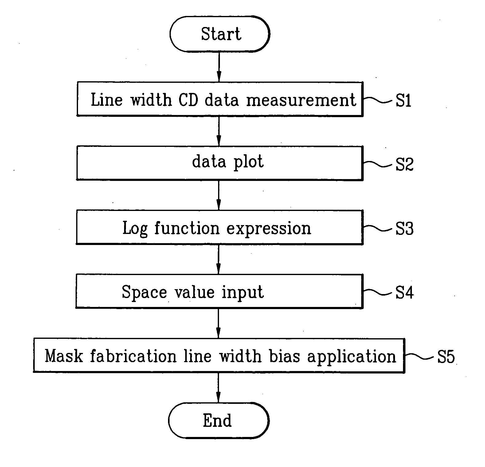
[0038]FIG. 3 is a flowchart of a method of calibrating a semiconductor line width according to an embodiment of the present invention.

[0039] Referring to FIG. 3, in design, fabrication, and correction of a mask, line width CD data adjusted by uniform interval are measured (S1), the measured line width CD data are selectively plotted according to a space size (S2), and the plotted measurement data values are then expressed by a log function (S3).

[0040] Subsequently, a space value is selectively inputted (S4) and an output value of the log function is then applied as a mask fabrication line width bias (S5).

[0041] Meanwhile, in the method of calibrating the semiconductor line width according to the embodiment of the prese...


PUM


Abstract

A method of calibrating a line width in a semiconductor device including fitting line width CD (critical dimension) data to a log function by measuring the line width CD data to plot selectively according to a space size in mask design, fabrication, and correction and applying an output value of the log function as a mask fabrication line width bias by selectively inputting a space value.

Description

BACKGROUND OF THE INVENTION [0001] 1. Field of the Invention [0002] The present invention relates to a method of calibrating a semiconductor line width, by which an irregular line width bias generated from exposure and etch in semiconductor fabrication is accurately corrected. [0003] 2. Discussion of the Related Art [0004] Generally, a photomask pattern directly affects the precision of a real pattern formed on a semiconductor substrate. If an optical proximity effect of the photomask pattern fails to be correctly taken into consideration, a pattern line width is distorted from the intended exposure of the photolithography. Hence, line width linearity is shortened, degrading the semiconductor device characteristics. [0005] In semiconductor photolithography, a precise design of a photomask enables a quantity of light transmitted via the photomask to be appropriately adjusted. For the precise design of the photomask, OPC, phase shift masking, and the like has been proposed, as well as...

Claims


Application Information

Patent Timeline
Patent Type & Authority Applications(United States)
IPC IPC(8): H01L21/027G06F17/50H01L21/66
CPCH01L22/12H01L21/027
Inventor LEE, JUN SEOK
Owner DONGBU ELECTRONICS CO LTD
Why Eureka
Try Eureka