Socket for testing a semiconductor device and a connecting sheet used for the same

a technology for semiconductor devices and sockets, which is applied in the field of sockets for testing semiconductor devices and the connection sheets used for the same. it can solve the problems of inability to test semiconductor devices, inability to arrange the probes b>1/b> of the conventional test socket, and inability to demonstrate the function of the socket, so as to achieve sufficient electric contact stably and continuously

Inactive Publication Date: 2005-07-07
MITSUBISHI ELECTRIC CORP
View PDF13 Cites 5 Cited by
  • Summary
  • Abstract
  • Description
  • Claims
  • Application Information

AI Technical Summary

Benefits of technology

[0013] It is an object of the present invention to solve the above-mentioned problems inherent in the conventional technique and to provide a test socket for semiconductor devices, which can stably and continuously realize sufficient electric contact between probes and outer connecting terminals.
[0030] According to a fifth aspect of the present invention, there is provided the test socket according to the fourth aspect of the invention, wherein the connecting sheet of the test socket has a connecting wire, which increases distances between the electrodes, being in contact with the outer connecting terminals of the semiconductor device, and is connected to the electrodes being in contact with the circuit board.

Problems solved by technology

Accordingly, it is difficult to arrange the probes 1 of the conventional test socket.
Therefore, a void is caused at time of mounting the outer connecting terminals to a printed circuit board and so on by melting the outer connecting terminals in use of reflow of solder, whereby a defect of blowhole is caused.
Further, as illustrated in FIG. 18, when remains 30 of solder adheres to and are deposited on a tip of a probe, the remains are oxidized in the atmosphere, and a contact resistance is increased by a coating of an oxide film 30a, there were problems that a semiconductor device could not be tested, and a function of the socket could not be demonstrated.
Further, there were problems that a contact resistance was increased by the coating of the oxide film, the semiconductor device could not be tested, and a function of the socket could not be demonstrated.
Further, it was necessary to spend a very long time and much labor for exchanging probes, selected as having high contact resistances or connection failures out of a large number, e.g. several hundreds, of the pin-like probes arranged in a grid-like form.
There was a problem that a cost becomes very high when a socket itself was changed because a unit price of the above-mentioned pin-like probe is high.

Method used


Image

  • Socket for testing a semiconductor device and a connecting sheet used for the same
  • Socket for testing a semiconductor device and a connecting sheet used for the same
  • Socket for testing a semiconductor device and a connecting sheet used for the same

Examples


embodiment 1

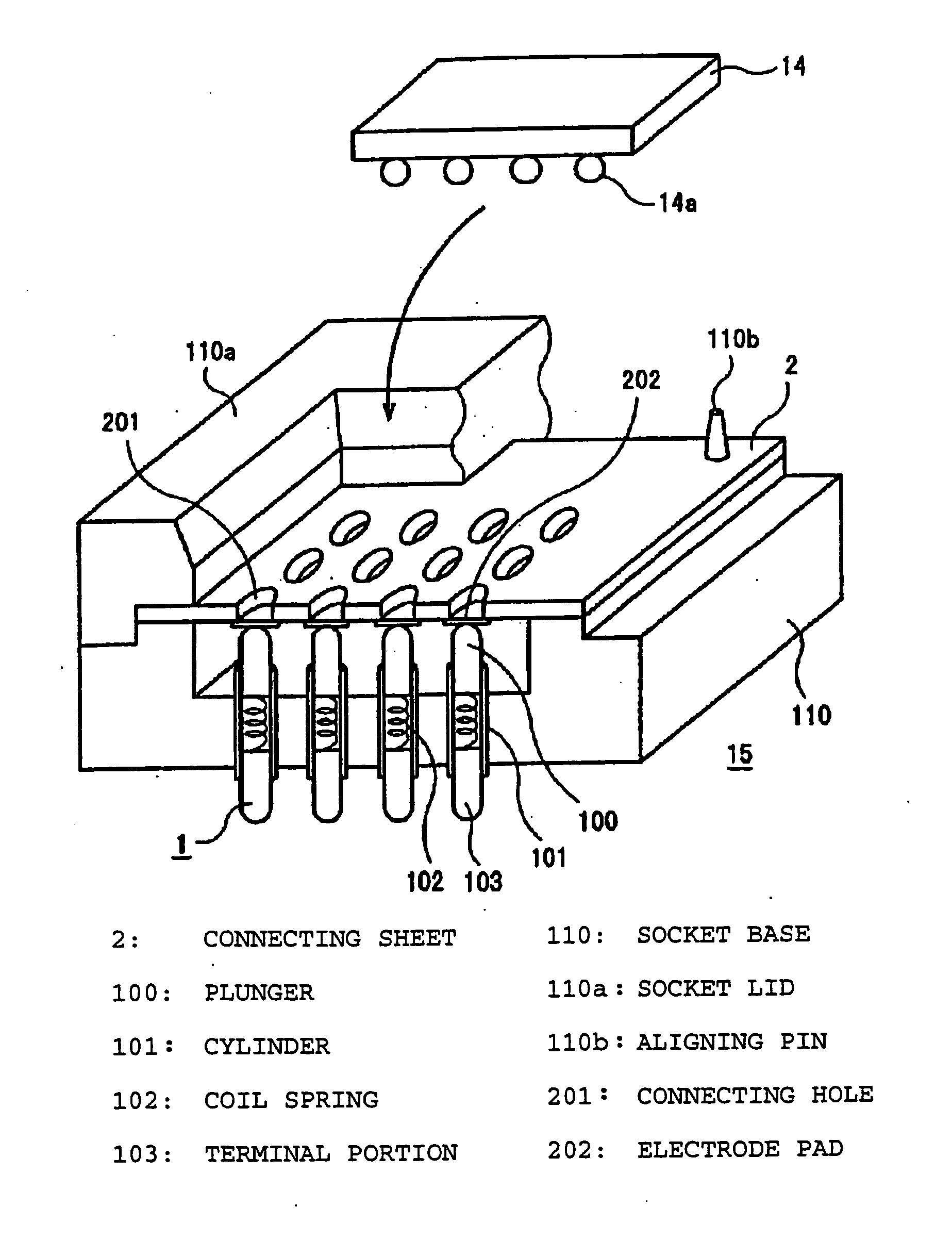
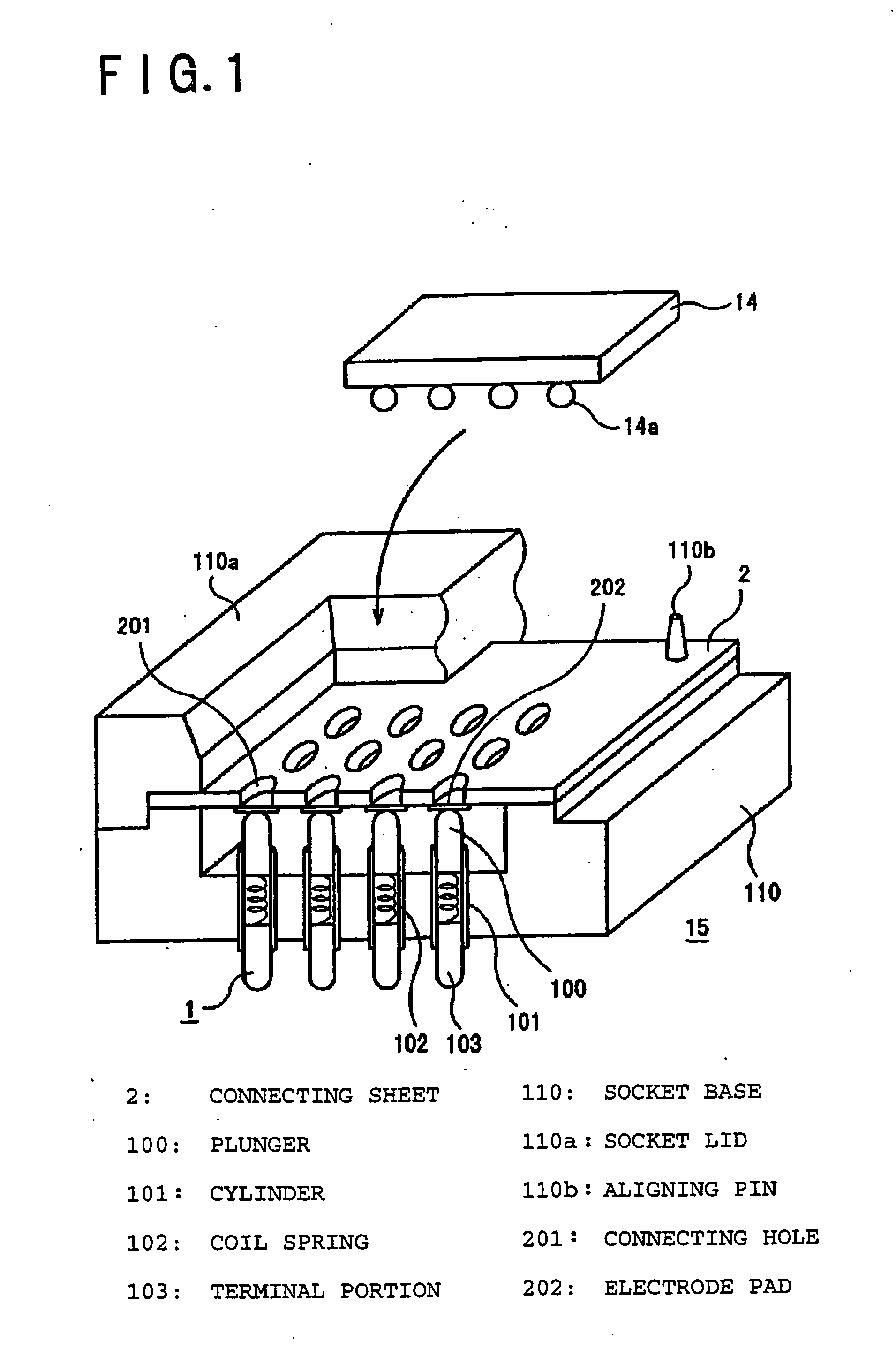
[0064]FIG. 1 is a perspective view illustrating a structure of a test socket according to Embodiment 1 of the present invention. In the figure, numerical reference 1 designates a probe; numerical reference 2 designates a connecting sheet; numerical reference 201 designates a connecting hole; numerical reference 202 designates an electrode pad; numerical reference 100 designates a plunger; numerical reference 101 designates a cylinder; numerical reference 102 designates a coil spring; numerical reference 103 designates a terminal portion, connected to a test board; numerical reference 110 designates a socket base; numerical reference 110a designates a socket lid; numerical reference 110b designates an aligning pin; numerical reference 14 designates a semiconductor package; numerical reference 14a designates an outer connecting terminal; and numerical reference 15 designates a socket.

[0065] In this test socket, an elastically deformative insulating member is used as a base, and the c...

embodiment 2

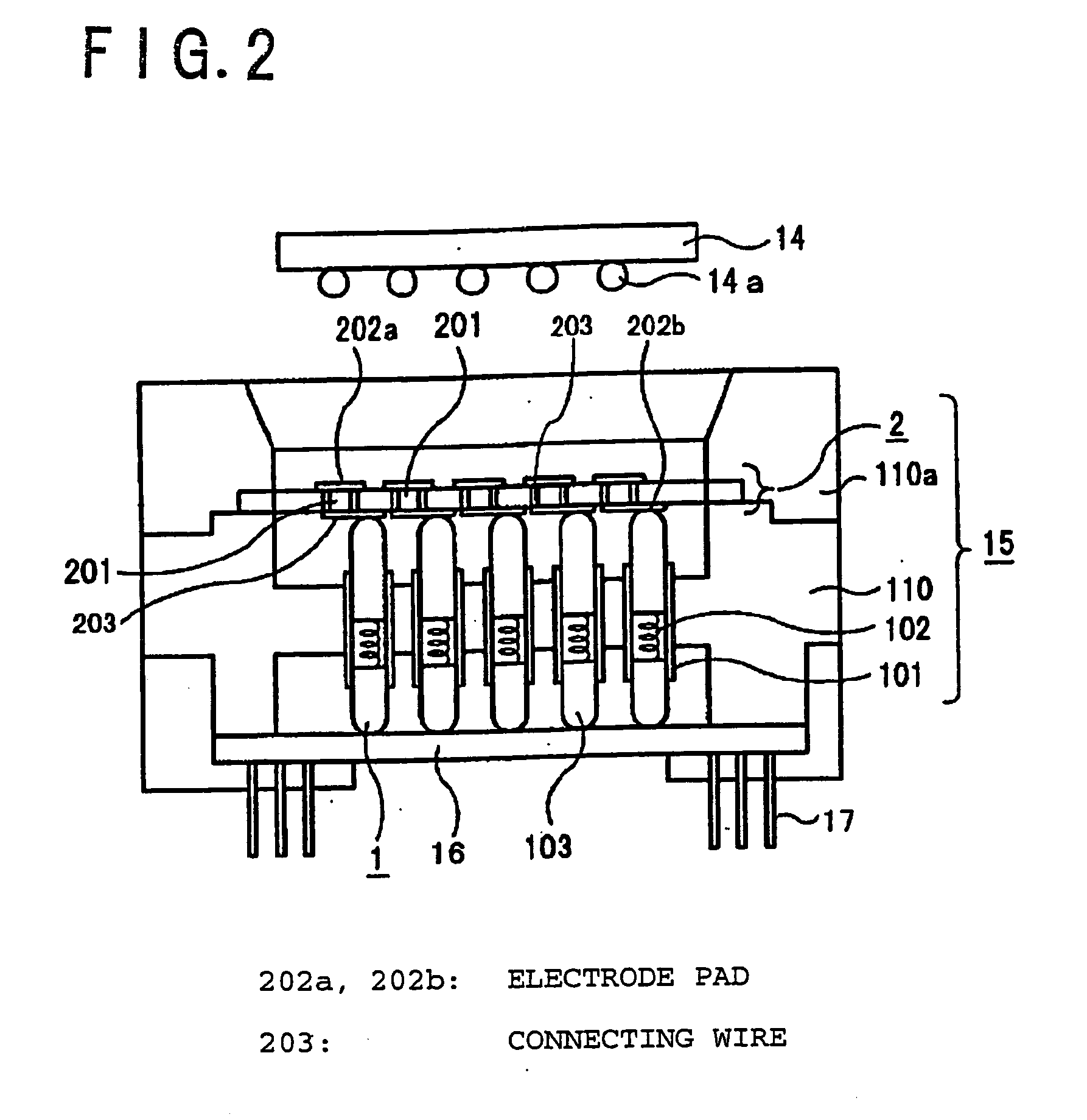
[0071]FIG. 2 is a cross-sectional view illustrating a structure of a test socket according to Embodiment 2 of the present invention. In the figure, numerical reference 1 designates a probe; numerical reference 2 designates a connecting sheet; numerical reference 201 designates a connecting hole; numerical references 202a and 202b designate electrode pads; numerical reference 203 designates a connecting wire; numerical reference 100 designates a plunger; numerical reference 101 designates a cylinder; numerical reference 102 designates a coil spring; numerical reference 103 designates a terminal portion; numerical reference 110 designates a socket base; numerical reference 110a designates a socket lid; numerical reference 14 designates a semiconductor package; numerical reference 14a designates an outer connecting terminal; numerical reference 15 designates a socket; numerical reference 16 designates a circuit board; and numerical reference 17 designates a connecting pin.

[0072] The c...

embodiment 3

[0074]FIG. 3 is a cross-sectional view illustrating a structure of a test socket according to Embodiment 3 of the present invention. In the figure, numerical reference 1 designates a probe; numerical reference 2 designates a connecting sheet; numerical reference 201 designates a connecting hole; numerical references 202a and 202b designate electrode pads; numerical reference 203 designates a connecting wire; numerical reference 204 designates a protrusion-like electrode; numerical reference 100 designates a plunger; numerical reference 100b designates a slit; numerical reference 101 designates a cylinder; numerical reference 102 designates a coil spring; numerical reference 103 designates a terminal portion; numerical reference 110 designates a socket base; numerical reference 110a designates a socket lid; numerical reference 14 designates a semiconductor package; numerical reference 14a designates an outer connecting terminal; numerical reference 15 designates a socket; numerical r...


PUM


Abstract

Probes 1 for testing and outer connecting terminals 14a are electrically connected to a-test socket for semiconductor devices. In use of a connecting sheet, fabricated by an elastically deformative insulating member and electrodes 202, flexibility is given, and good electrical contacts are obtainable. Further, because the connecting sheet 2 is exchangeable, contacting capability is recovered by exchange when solder debris is adhered and deposited to increase contact resistances. Accordingly, even though there is scattering of the heights of the outer connecting terminals, good electrical contact with the probes is obtainable, and even though the solder debris of the outer connecting terminals is adhered and deposited as a result of repeated usage, tests can be continuously conducted, wherein the test socket for semiconductor devices has good maintenance capability.

Description

[0001] This application is a divisional of application Ser. No. 10 / 659,281, filed on Sep. 11, 2003, which is a continuation of application Ser. No. 09 / 686,981, filed on Oct. 17, 2000 (now abandon).FIELD OF THE INVENTION [0002] The present invention relates to a test socket used for testing electrical characteristics of semiconductor devices. DISCUSSION OF BACKGROUND [0003] In accordance with advancement of functions and miniaturization of electronic equipments, the number of outer connecting terminals of semiconductor devices are increased, a density of semiconductor device becomes high, and semiconductor packages such as a ball grid array (BGA) type, which is formed by arranging outer connecting terminals on a lower surface of a semiconductor device in a grid-like form, and a chip scale package (CSP) type are increasingly used instead of a QFP type formed by arranging outwardly drawn-out connecting terminals, or an SOP type semiconductor package. When such a semiconductor package i...

Claims


Application Information

Patent Timeline
Patent Type & Authority Applications(United States)
IPC IPC(8): G01R31/26G01R1/04G01R31/02
CPCG01R1/0483
Inventor MAEKAWA, SHIGEKIKASHIBA, YOSHIHIRO
Owner MITSUBISHI ELECTRIC CORP
Why Eureka
Try Eureka