Method and system for monitoring IC process

Inactive Publication Date: 2005-07-14
HERMES-MICROVISION INC
View PDF22 Cites 15 Cited by
  • Summary
  • Abstract
  • Description
  • Claims
  • Application Information

AI Technical Summary

Benefits of technology

[0017] Many benefits are achieved by way of the present invention over conventional techniques. For example, some embodiments of the present invention provide a semiconductor wafer measurement and inspection technique to accurately monitor and visualize processing conditions such as uniformity or variation of particular processes within a die, within a wafer, between wafers within a lot, and/or between lots. Certain embodiments of the present invention provide contour maps representing average grayscale values for the background, average grayscale values for processed features, and adjusted grayscale values. These two-dimensional contour maps can serve as reliable indicators of overall process conditions across an entire wafer and/or between wafers. Some embodiments of the present invention provide quick visual representation using sample region images as well as grayscale values for the processed features and the background. For example, the visual representation takes the form of contour plots and clearly shows wafer level variations. Certain embodiments of the present invention use sample regions within a die to determine process uniformity within a die or designated sample regions within a wafer to determine the process uniformity within a wafer. Some embodiments of the present invention enable a process engineer to get a quick synopsis of the process performance across the wafer, supported by statistically quantitative measures. For example, a lot of data can be generated by e-beam inspection, which may be highly voluminous to handle and thereby making its significance difficult to understand. With quick visualization and comparative analysis of the data in a concise manner, appropriate process corrections can be made in a timely manner. As another example, it is important to identify process equipment lifetime issues and limitations as soon as p

Problems solved by technology

Integrated circuit (IC) processing has become increasingly challenging as feature sizes continue to shrink.
Shrinking dimensions and increasing wafer sizes are making the maintenance of process uniformity throughout the wafer important but difficult to attain.
Process windows are rapidly narrowing in advanced wafer manufacturing, and process variations can happen as inadequate time is spent to perfect the process due to the economic pressure of higher average selling price for the latest technology.
Spatial variation across the wafer results from equipment or process disturbances or limitations.
Making too few measurements may be inadequate whereas making too many measurements can make the data collection and processing unnecessarily tedious.
Wafer-level variation is often characterized by low spatial frequency trends that are caused by equipment design and/or operation limitations.
With advanced semiconductor manufacturing technology, the etch process for high aspect ratio structures, e.g., contact and/or via holes in dual damascene, has become increasingly challenging due to

Method used


Image

  • Method and system for monitoring IC process
  • Method and system for monitoring IC process
  • Method and system for monitoring IC process

Examples


Example

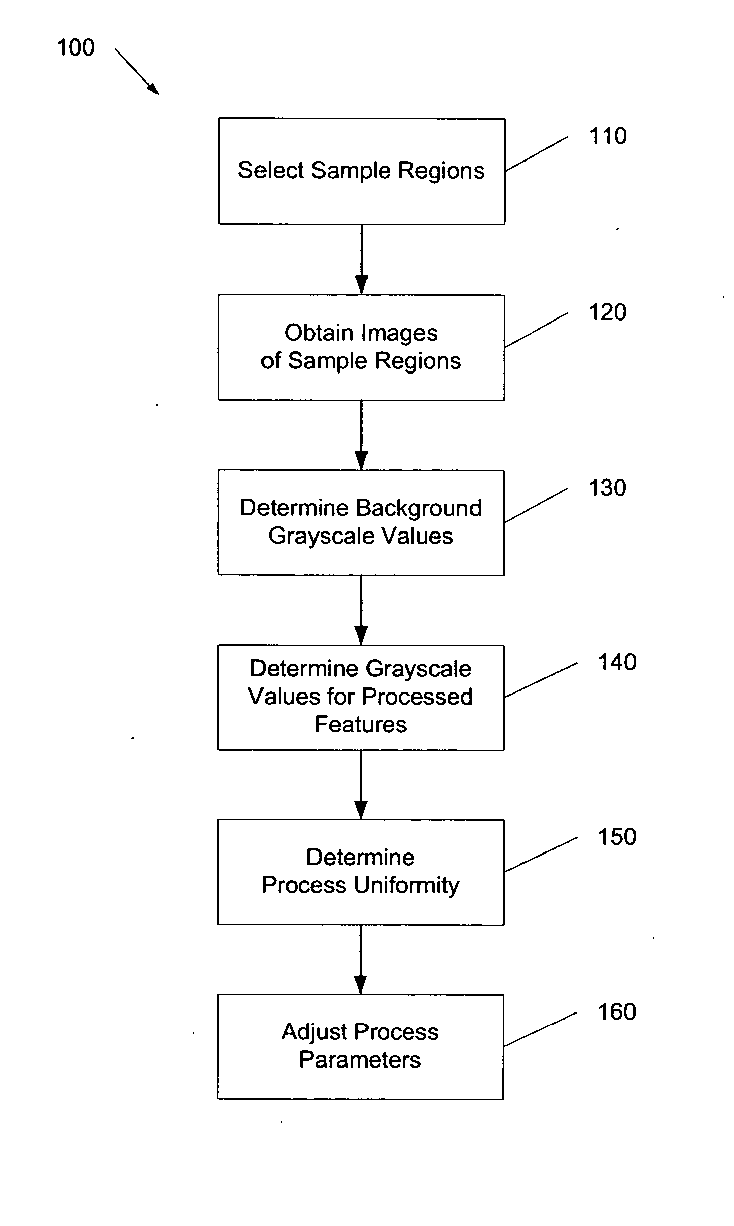
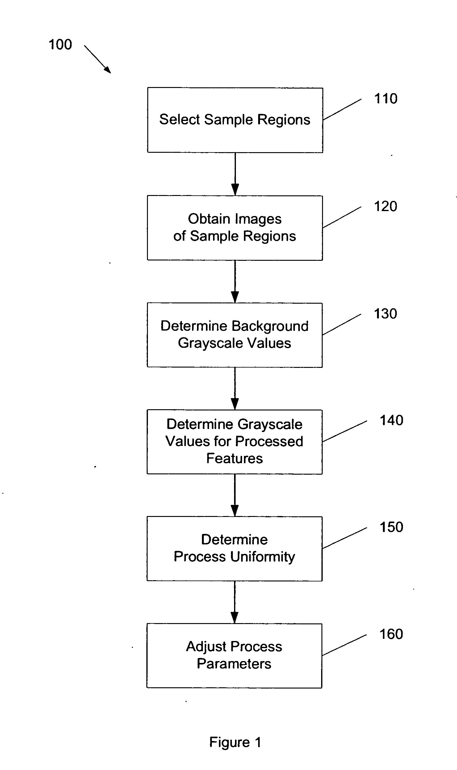
[0031] The present invention is directed to integrated circuit (IC) fabrication. More particularly, the invention provides a method and system for examining IC process uniformity. Merely by way of example, the invention has been applied to inline monitoring. But it would be recognized that the invention has a much broader range of applicability.

[0032]FIG. 1 is a simplified method for monitoring IC process uniformity according to an embodiment of the present invention. This diagram is merely an example, which should not unduly limit the scope of the claims. One of ordinary skill in the art would recognize many variations, alternatives, and modifications. A method 100 includes a process 110 for selecting sample regions, a process 120 for obtaining images of sample regions, a process 130 for determining background grayscale values, a process 140 for determining grayscale values for processed features, a process 150 for determining process uniformity, and a process 160 for adjusting pr...


PUM


Abstract

A method and system for determining process uniformity. The method includes selecting a plurality of sample regions. The plurality of sample regions includes a plurality of processed features, and each of the plurality of sample regions includes at least one of the plurality of processed features. Each of the plurality of processed features results from at least one fabrication process. Additionally, the method includes obtaining a plurality of electron microscope images associated with the plurality of sample regions respectively, processing information associated with the plurality of electron microscope images, and, determining a first plurality of grayscale values for the plurality of sample regions respectively. Moreover, the method includes processing information associated with the first plurality of grayscale values, and determining whether the at least one fabrication process is uniform.

Description

CROSS-REFERENCES TO RELATED APPLICATIONS [0001] This application claims priority to U.S. Provisional No. 60 / 518,865, filed Nov. 10, 2003, which is incorporated by reference herein for all purposes.STATEMENT AS TO RIGHTS TO INVENTIONS MADE UNDER FEDERALLY SPONSORED RESEARCH OR DEVELOPMENT [0002] NOT APPLICABLE REFERENCE TO A “SEQUENCE LISTING,” A TABLE, OR A COMPUTER PROGRAM LISTING APPENDIX SUBMITTED ON A COMPACT DISK. [0003] NOT APPLICABLE BACKGROUND OF THE INVENTION [0004] The present invention is directed to integrated circuit (IC) fabrication. More particularly, the invention provides a method and system for examining IC process uniformity. Merely by way of example, the invention has been applied to inline monitoring. But it would be recognized that the invention has a much broader range of applicability. [0005] Integrated circuit (IC) processing has become increasingly challenging as feature sizes continue to shrink. Shrinking dimensions and increasing wafer sizes are making th...

Claims


Application Information

Patent Timeline
IPC IPC(8): H01L21/66G06K9/00G06T7/00H01L21/00H01L21/02H01L21/3205H01L23/52
CPCG06T7/0004H01L21/67288G06T2207/30148
Inventor JAU, JACKSUNDARARAJAN, SRINIVASAN
Owner HERMES-MICROVISION INC
Why Eureka
Try Eureka