Semiconductor device

a technology of semiconductor devices and semiconductors, applied in the direction of semiconductor devices, semiconductor/solid-state device details, diodes, etc., can solve the problems of causing deterioration in s/, generating circuit noise, spurious noise, etc., and achieving the effect of preventing deterioration in characteristics

Inactive Publication Date: 2005-07-21
PANASONIC CORP
View PDF7 Cites 20 Cited by
  • Summary
  • Abstract
  • Description
  • Claims
  • Application Information

AI Technical Summary

Benefits of technology

[0021] The present invention provides a semiconductor device in which an analog circuit block and a digital circuit block are combined and which is c

Problems solved by technology

Those circuits generate divided waves and higher harmonic waves of the high-frequency signal and the local oscillation signal, and also generate circuit noise.
In consequence, the related art semiconductor device have had a problem that unwanted noise and spurious have occurred in the circuit output signals of other circuit blocks to induce deterioration in the S/N (Signal/Noise) and the C/N (Carrier/Noise) of their signals and desensitization to input signals of the circuits.
As a result, spurious and noise having frequency bands used for transmission and reception occur to induce deterioration in characteristics, such as deterioration in the S/N and the C/N of t

Method used


Image

  • Semiconductor device
  • Semiconductor device
  • Semiconductor device

Examples


embodiment 1

(Embodiment 1)

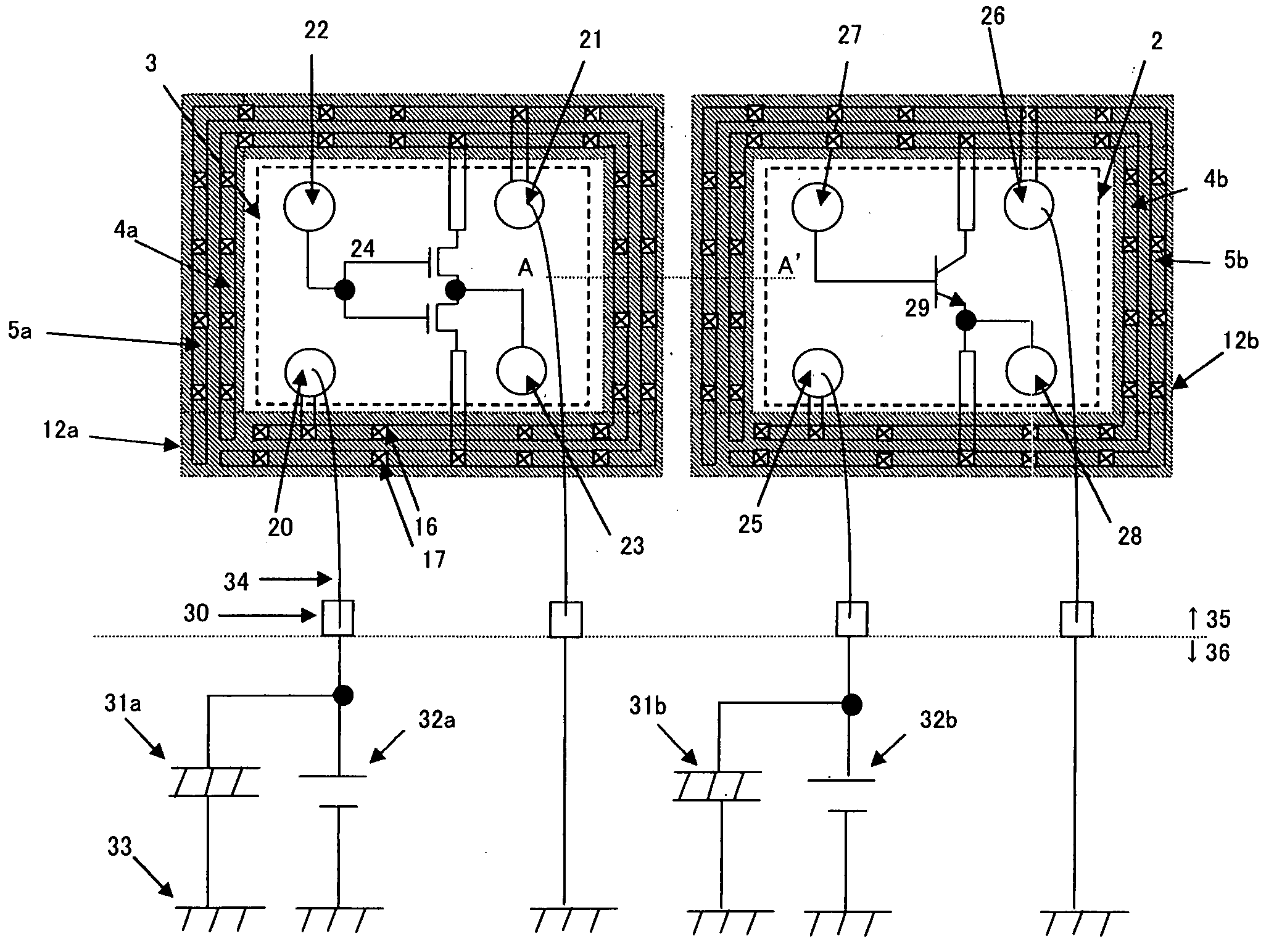
[0048] In Embodiment 1, a semiconductor device in which a digital circuit block and an analog circuit block are combined on one and the same semiconductor substrate is explained with reference to FIG. 1. The outside shape of its IC substrate is not shown in FIG. 1.

[0049] With this semiconductor device, a digital circuit region 3 and an analog circuit region 2 are adjacent to each other and are independently placed as shown in FIG. 1. In the digital circuit region 3, a digital circuit block is constituted by placing MOS transistors 24 and so on. In the analog circuit region 2, an analog circuit block is constituted by placing a bipolar transistor 29 and so on.

[0050] Around the digital circuit region 3, a digital circuit power supply wiring 4a and a digital circuit ground wiring 5a, which are connected to the elements in the digital circuit region 3, are placed. The digital circuit power supply wiring 4a and the digital circuit ground wiring 5a have a gap at a place on...

embodiment 2

(Embodiment 2)

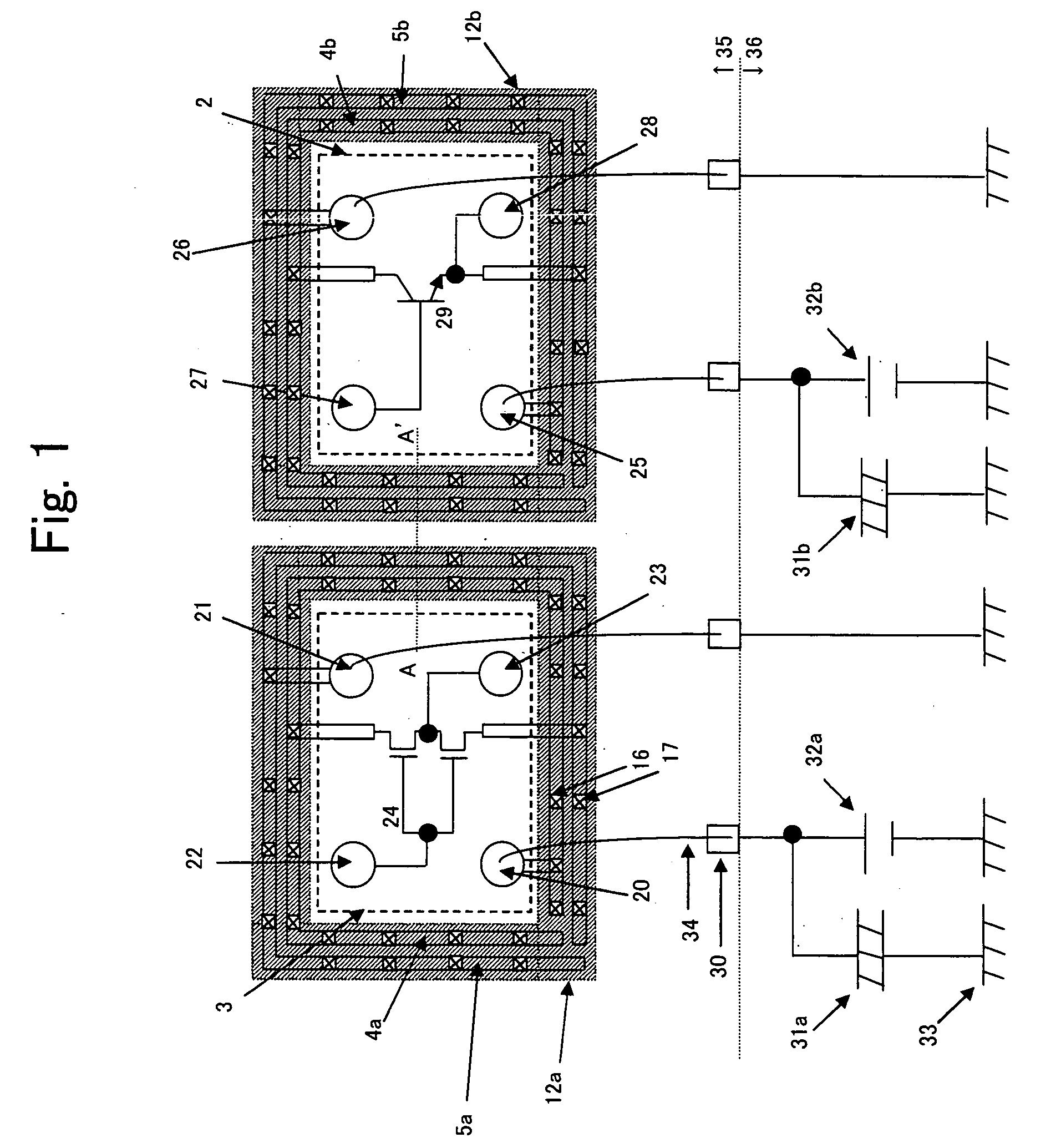
[0067] Next, Embodiment 2 will be explained with reference to FIG. 3. In a semiconductor device shown in FIG. 3, a digital circuit region 3 and an analog circuit region 2 are adjacent to each other and are independently placed. In the digital circuit region 3, a digital circuit is constituted by placing MOS transistors 24 and so on. In the analog circuit region 2, an analog circuit is constituted by placing a bipolar transistor 29 and so on.

[0068] Around the circuit regions 3 and 2, a digital circuit power source wiring 4a, a digital circuit ground wiring 5a, an analog circuit power source wiring 4b, and an analog circuit ground wiring 5b, which are connected to the elements in the circuit regions 3 and 2 respectively, are placed in such a manner that they have a gap at a place on the periphery of the circuit regions 3 and 2.

[0069] In FIG. 3, the outside shape of the IC substrate is not shown. Also, in this embodiment, the digital circuit power supply wiring 4a and t...


PUM


Abstract

There is provided a semiconductor device, wherein a digital circuit region and an analog circuit region are located independently. A power supply wiring and a ground wiring are placed on the periphery of each circuit region and are connected to elements in each circuit region. A MOS capacitor is formed under the power supply wiring and the ground wiring. The terminals of the MOS capacity are connected to the power supply wiring and the ground wiring. Pads are placed in each circuit region surrounded by the power supply wiring, the ground wiring, and the MOS capacitor and are connected to the elements of each circuit region.

Description

BACKGROUND OF THE INVENTION [0001] 1. Field of the Invention [0002] The present invention relates to a semiconductor device. More particularly, the present invention relates to a semiconductor device which takes measures against interference and noise between circuit blocks in a semiconductor integrated circuit in which an analog circuit block and a digital circuit block are combined on a single chip. [0003] 2. Background Art [0004] With the recent popularity of semiconductor integrated circuit devices having larger packing densities and higher performance, an integrated circuit used for cellular phones and so on has been intended to have a structure that a plurality of analog and digital circuits, such as a transmitting circuit, a receiving circuit, and a PLL circuit, are combined on one and the same substrate through the use of BiCMOS process technology. [0005] Such an integrated circuit generally receives a signal of 10 to 30 MHZ from an external temperature-compensated crystal o...

Claims


Application Information

Patent Timeline
IPC IPC(8): H01L21/822H01L23/522H01L23/528H01L27/04H01L27/06H01L27/08H01L29/94
CPCH01L23/5223H01L23/5286H01L2924/1305H01L2924/13091H01L2924/01033H01L24/48H01L2924/3025H01L2924/3011H01L2924/30105H01L24/49H01L27/0635H01L27/0811H01L29/94H01L2224/48091H01L2224/49H01L2924/01004H01L2924/01005H01L2924/01006H01L2924/01013H01L2924/01015H01L2924/01082H01L2924/14H01L2924/19041H01L2924/00014H01L2924/00H01L2224/45099H01L2224/05599
Inventor NAKANO, HIDEOYOSHIDA, SHOJIMAEDA, MASAKATSU
Owner PANASONIC CORP
Why Eureka
Try Eureka