Semiconductor device and method of its manufacture

a semiconductor and device technology, applied in the direction of semiconductor devices, basic electric elements, electric devices, etc., can solve the problems of high contamination risk, high cost, and large number of highly complex and expensive machines, and achieve the effect of reducing the requirement of “clean room” and simplifying and improving the accuracy of delivery

Inactive Publication Date: 2005-07-21
PALTI YORAM
View PDF7 Cites 6 Cited by
  • Summary
  • Abstract
  • Description
  • Claims
  • Application Information

AI Technical Summary

Benefits of technology

[0011] There is a need in the art to facilitate manufacture of semiconductor devices by providing a novel manufacturing method which provides for reducing the features' size (the co-called “critical dimensions”), eliminating the need for or at least significantly reducing the “clean room” requirements, and eliminating the need for using a mask in a lithography process. There is also a need for a chip manufacturing technique simplifying the vacuum-based layer deposition process (CVD or PVD), as well as providing a simpler and more accurate means for delivering controlling and changing fluids associated with various fabrication processes and providing better means for mechano-chemical polishing.

Problems solved by technology

These processes are carried out by means of numerous highly complex and expensive machines.
These processes generate dirt-dust particles and are highly susceptible to contamination by such particles as well as ones originating from the environment and workforce.
One of the basic critical, time consuming processes, requiring extremely high accuracy (that determines the quality of the product) and very expensive machinery is the lithography.
On the whole this is time consuming and requires large volumes of chemicals, etc.

Method used


Image

  • Semiconductor device and method of its manufacture
  • Semiconductor device and method of its manufacture
  • Semiconductor device and method of its manufacture

Examples


Embodiment Construction

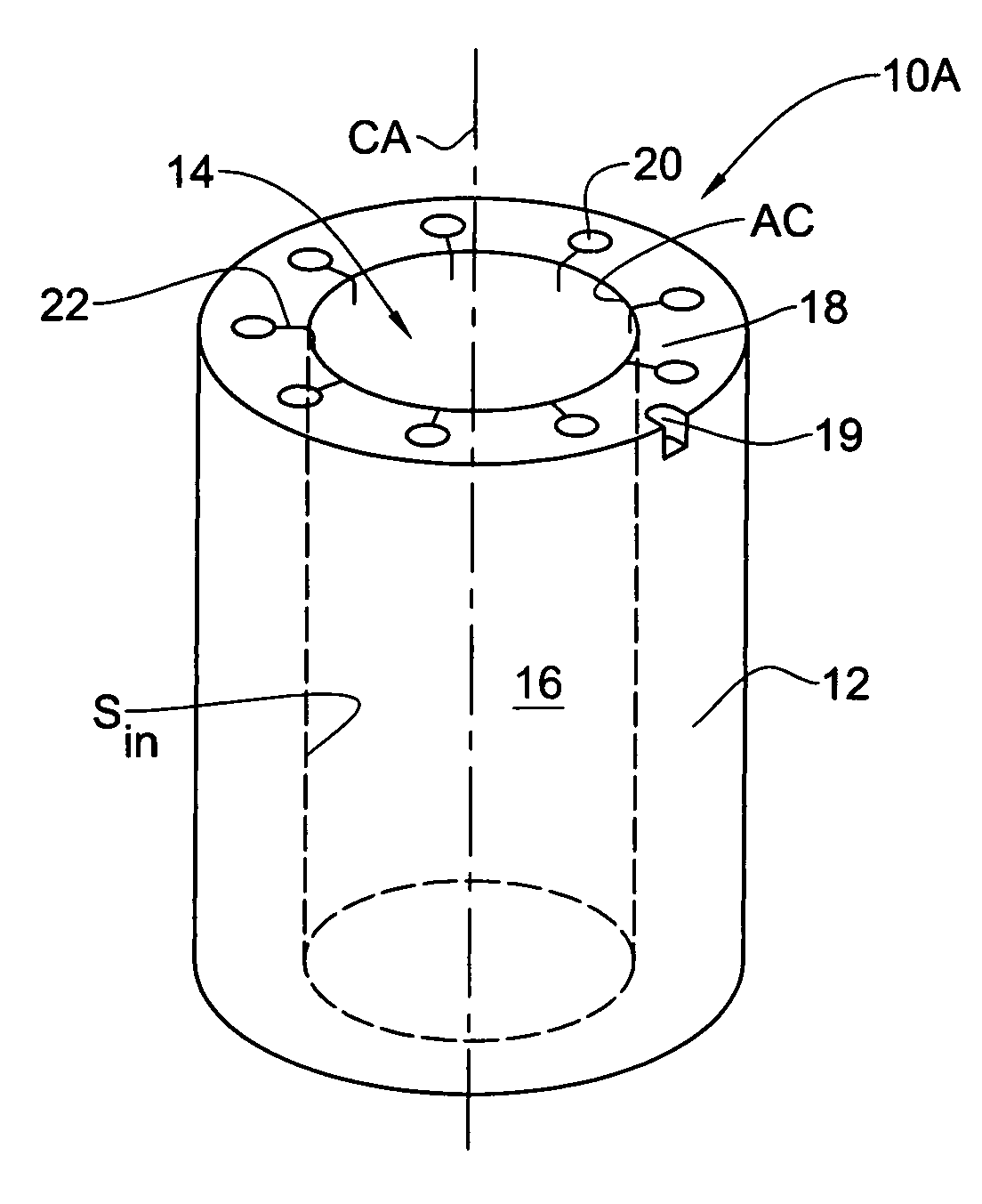
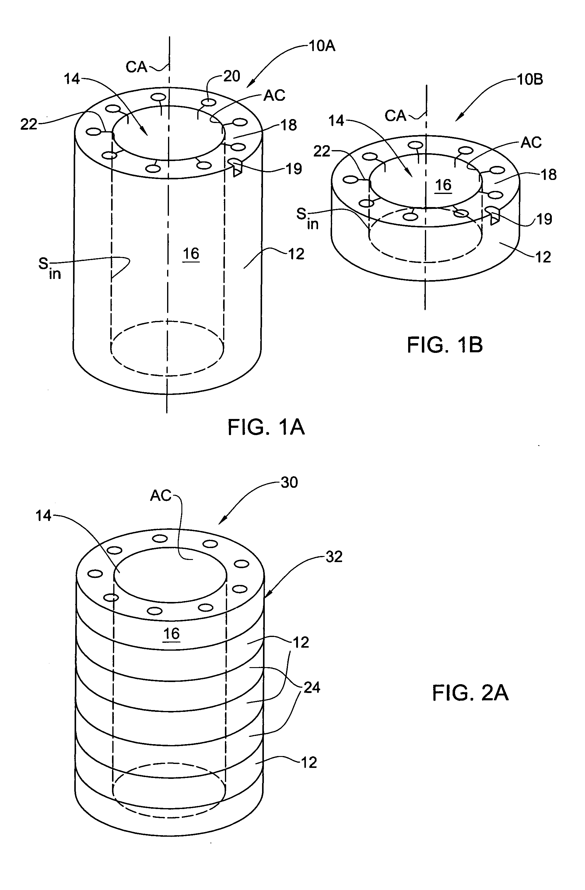
[0050] Referring to FIGS. 1A and 1B, there are schematically illustrated two examples, respectively, of an integrated semiconductor device or part thereof (generally, a chip) according to the invention. In the example of FIG. 1A, a device 10A has an elongated tubular-like configuration (its height is larger than its width), while in the example of FIG. 1B, a device 10B has a ring-like geometry (its height is smaller than its width). To facilitate understanding, the same reference numbers are used to identify common components in all the examples of the invention. These semiconductor devices are configured as annular chips AC.

[0051] The semiconductor device 10A (or 10B) includes a semiconductor element (wafer) 12 carrying electronic elements (features) of the semiconductor device, which are typically produced as a patterned area in the semiconductor element. The semiconductor element 12 has a through-going opening (perforation) 14 extending along a central axis CA thereof. This perf...


PUM


Abstract

An integrated semiconductor device and method for its manufacturing are presented. A semiconductor element is provided having a perforation extending along a central axis of the element, thereby defining a central channel inside said element. An inner surface of the perforation is processed via the central channel to define features of the semiconductor device to be manufactured.

Description

FIELD OF THE INVENTION [0001] This invention relates to semiconductor devices and method of manufacturing such devices. BACKGROUND OF THE INVENTION [0002] In accordance with the existing technology, semiconductor devices (microchips) are planar, basically rectangular units containing multiple electronic elements (logic switches, gates, etc.) and circuitry often arranged in multiple layers. The microchips are manufactured in a very elaborate multi-stage process on semiconductor wafers, typically thin silicone discs of 10-20 cm in diameter. A wafer structure usually contains numerous small discrete electronic units (chips), many or all of which are identical. Unit size may be about 0.1-1.0 cm2. Thus, a wafer structure may contain hundreds to thousands of individual electronic units. [0003] The main processes involved in the chip manufacture are as follows: lithography, wet processing, washing, rinsing, etc.; thermal processing; Chemical Vapor Deposition (CVD); Physical Vapor Depositio...

Claims


Application Information

Patent Timeline
Patent Type & Authority Applications(United States)
IPC IPC(8): H01L21/027H01L29/06
CPCH01L29/0657H01L21/0271
Inventor PALTI, YORAM
Owner PALTI YORAM
Why Eureka
Try Eureka