Nanostructures with electrodeposited nanoparticles

a nanoparticle and nanostructure technology, applied in the field of electrodeposited nanostructures, can solve the problems of limited nanostructure approaches, difficult modification effects, and limited nanostructures, and achieve the effect of reducing the size of the minimum size of the region, and reducing the size of the nanostructur

Inactive Publication Date: 2005-07-21
NANOMIX
View PDF22 Cites 50 Cited by
  • Summary
  • Abstract
  • Description
  • Claims
  • Application Information

AI Technical Summary

Benefits of technology

[0011] The geometry of the nanostructures in the nanoelectronic devices on the substrate may be used to create different types of deposition patterns. For example, in an embodiment of the invention, nanoparticles with different chemical compositions may be caused to form clusters of nanoparticles at particular locations on the nanostructures. In the alternative, or in addition, different materials may be deposited in nanoparticles having a layered structure, with each layer comprising a different material. A further variation is to form nanoparticles of different materials in different regions of a nanostructure film or other structure. Since all of the materials can be localized to the nanostructures using a method according to the invention, the substrate may remain substantially unaffected by deposition of the nanoparticles.

Problems solved by technology

However, these modifications can be difficult to effect.
This approach is limited to those nanostructures which can be readily put into solution.
These particles coat the substrate and the nanostructures uniformly, which may be undesirable for some applications.
But the minimum size of these regions is limited by the techniques of lithography, and within these regions the particle coatings are uniform.
A exemplary problem arises by the incorporation of nanotubes into electronic devices for use as hydrogen sensors.
However, the uniformity of the coating within lithographically-definable regions of minimum size prevents the electronic devices from operating as transistor-type sensors.

Method used


Image

  • Nanostructures with electrodeposited nanoparticles
  • Nanostructures with electrodeposited nanoparticles
  • Nanostructures with electrodeposited nanoparticles

Examples


example 1

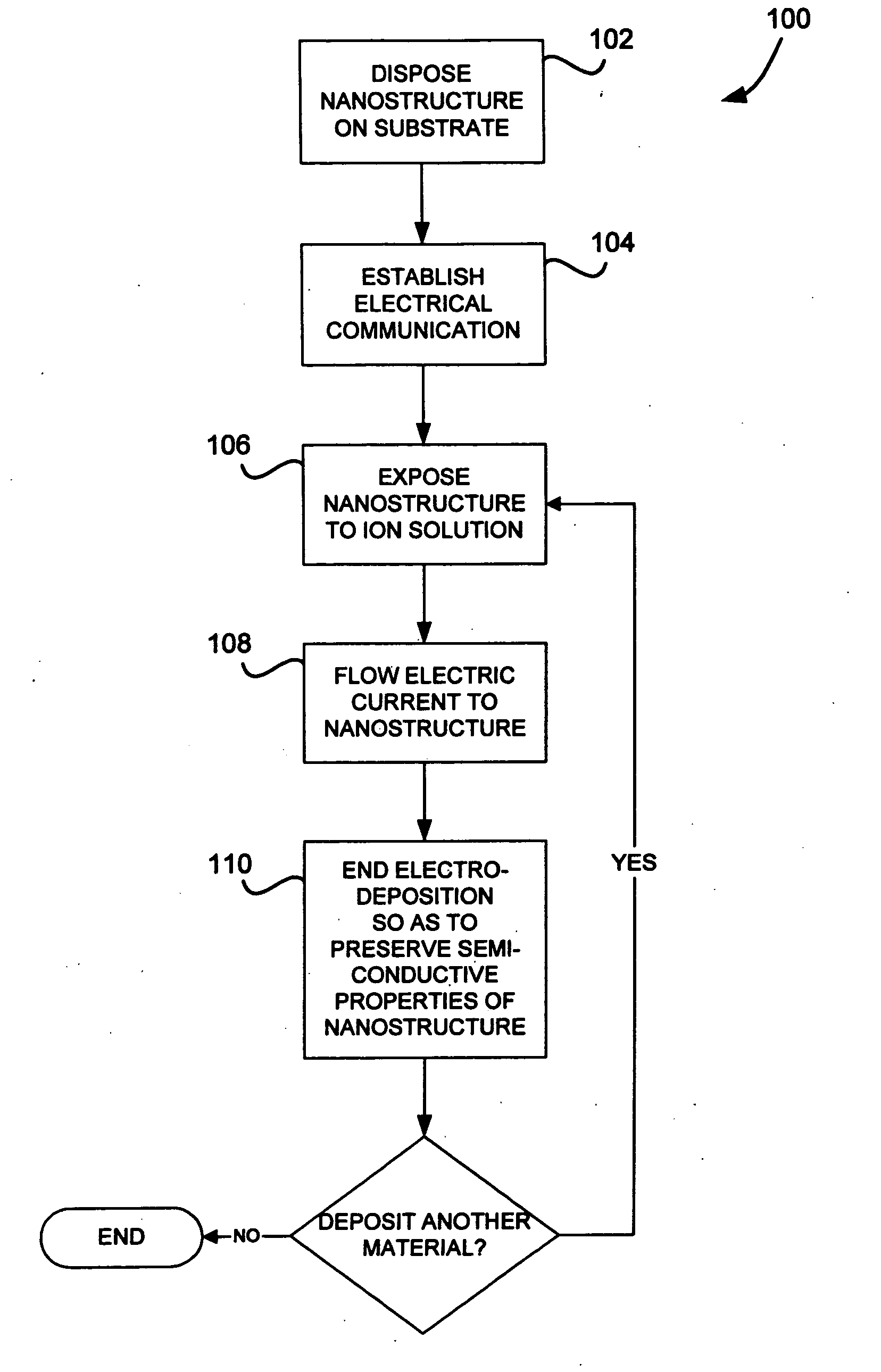
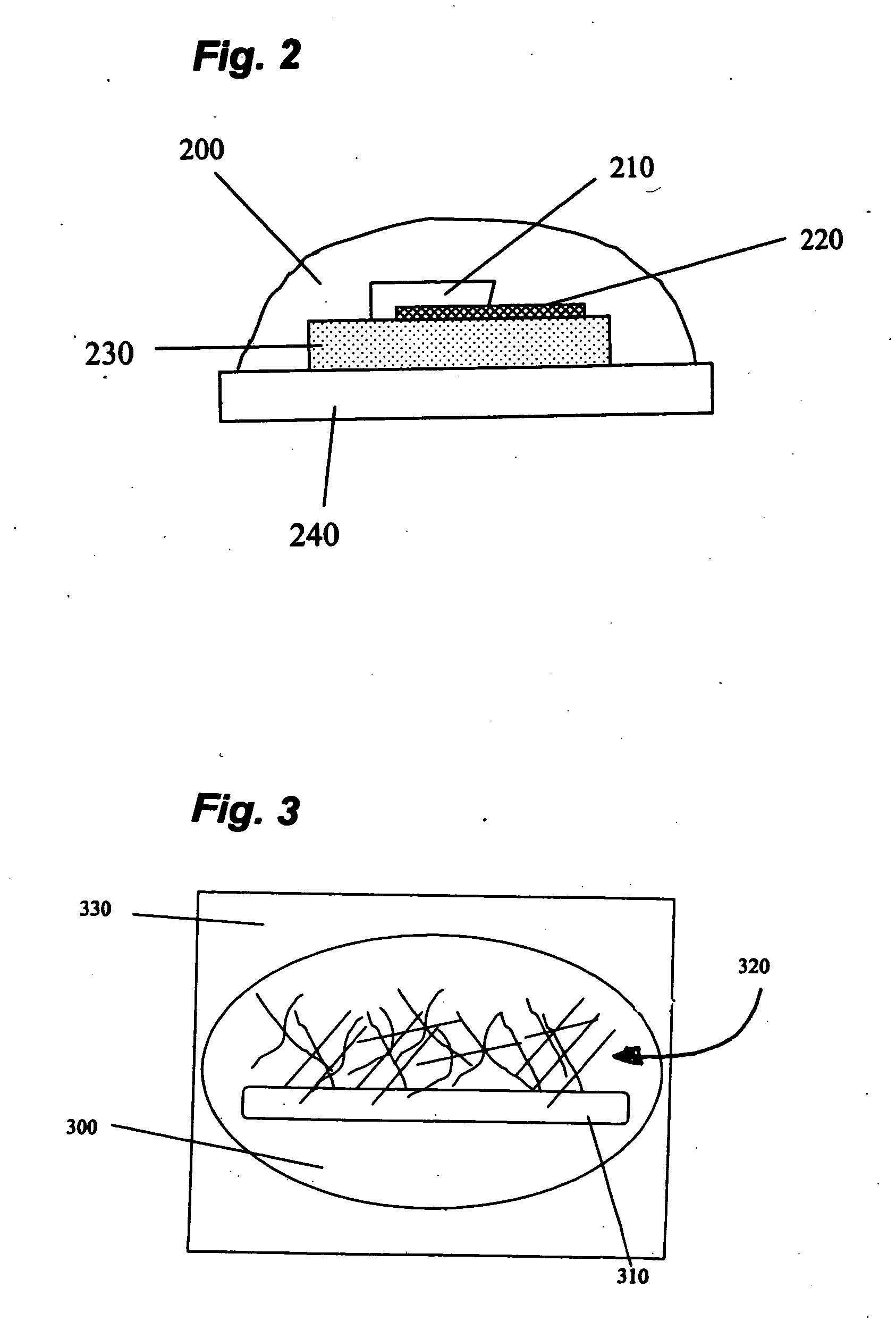
[0047] A nanotube network was prepared as described in U.S. application Ser. No. 10 / 177,929. A titanium film was deposited by evaporation and patterned lithographically into the form of electrical contacts. The substrate was placed on an aluminum block, this block being electrically grounded. Copper and iron blocks were also used for some experiments. Metal pins were pushed onto several of the titanium contacts on the substrate, thus making electrical contact. These metal pins were electrically grounded. The chip was rinsed with a 1:1 mixture of water and ethanol for cleaning. A 5 mM solution of PdCl2 in a 1:1 mixture of water and ethanol was prepared. Five drops of the solution were placed on the substrate, with the solution contacting both the substrate and the underlying aluminum block. After 30 seconds, the solution was rinsed off with a 1:1 mixture of water and ethanol, and the chip was dried with a stream of compressed air. Subsequently, a 5 mM solution of Na3RhCl6 in a 1:1 mi...

example 2

[0050] A nanotube network was prepared like that of Example 1. An aluminum (or other possible counterelectrode metal) film (50 nm) was deposited by evaporation and patterned lithographically into the form of electrical contacts. The chip was rinsed with a 1:1 mixture of water and ethanol for cleaning. The chip was then submerged in a vial of ˜1 mL 5 mM PdCl2 solution in a 1:1 mixture of water and ethanol. After 30 seconds, the chip was removed from the vial and the solution was rinsed off with a 1:1 mixture of water and ethanol. Finally, the chip was dried with a stream of compressed air. Subsequently, a 5 mM solution of Na3RhCl6 in a 1:1 mixture of water and ethanol was prepared. The chip was then submerged in ˜1 mL of the Na3RhCl6 solution. After 30 seconds, the solution was rinsed off with a 1:1 mixture of water and ethanol, and the chip was dried with a stream of compressed air.

example 3

[0051] Application of an electrodeposition process to fabrication of multi-analyte sensor arrays was demonstrated. The finished sensor arrays were tested by passing different analytes over the sensor array and resolving signatures for the given gases, thereby identifying them. In a laboratory setting, various gases were delivered to the surface of the sensor array. Response data was collected and analyzed using a technique for negate the bias associated with poisoning and nonrandom sampling. The data stream was then filtered and processed through principal component analysis (PCA) to recognize the signature associated with each gas analyte.

[0052] Site-specific metal electrodeposition was used to deposit nanoparticles of different composition on different regions of nanotube films in adjacent sensor devices on a chip. Adjacent devices were thereby functionalized to respond to different analytes. Control of the electrodeposition process was accomplished by grounding specific nanotube...


PUM

PropertyMeasurementUnit
currentaaaaaaaaaa
currentaaaaaaaaaa
timeaaaaaaaaaa

Abstract

A nanoelectronic device includes a nanostructure, such as a nanotube or network of nanotubes, disposed on a substrate. Nanoparticles are disposed on or adjacent to the nanostructure so as to operatively effect the electrical properties of the nanostructure. The nanoparticles may be composed of metals, metal oxides, or salts, and nanoparticles composed of different materials may be present. The amount of nanoparticles may be controlled to preserve semiconductive properties of the nanostructure, and the substrate immediately adjacent to the nanostructure may remain substantially free of nanoparticles. A method for fabricating the device includes electrodeposition of the nanoparticles using one or more solutions of dissolved ions while providing an electric current to the nanostructures but not to the surrounding substrate.

Description

CROSS-REFERENCE TO RELATED APPLICATION [0001] This application claims priority pursuant to 35 U.S.C. § 119(e) to U.S. Provisional Application Number 60 / 504,663, filed Sep. 18, 2003, which application is specifically incorporated herein, in its entirety, by reference.BACKGROUND OF THE INVENTION [0002] 1. Field of the Invention [0003] The present invention relates to electrical devices using nanostructures, for example, nanotubes or nanowires, as a conductive element. [0004] 2. Description of Related Art [0005] Electronic devices using nanostructures as electrical conductors are useful as transistors, optoelectronic devices, and chemical and biological sensors. Nanostructures that have been used in such devices include carbon nanotubes and silicon nanowires. For a variety of reasons, it is desirable to modify the nanostructures. Modified nanostructures can have improved electrical characteristics, greater sensitivity to chemicals, or greater specificity in their sensitivity to chemica...

Claims


Application Information

Patent Timeline
Patent Type & Authority Applications(United States)
IPC IPC(8): G01N27/00G01N27/414G01N33/00
CPCB82Y30/00Y10S977/72G01N33/005G01N27/4146C25D3/12C25D3/46C25D3/48C25D3/50C25D5/02C25D5/10C25D5/54C25D17/005C25D21/12
Inventor BRADLEY, KEITHDAVIS, ALONA J.GABRIEL, JEAN-CHRISTOPHE P.HAN, TZONG-RUJOSHI, VIKRAMSTAR, ALEXANDER
Owner NANOMIX
Why Eureka
Try Eureka