Organic electroluminescent element and lumiscent device or display including the same

a lumiscent device and electroluminescent element technology, applied in the direction of discharge tube luminescnet screens, other domestic articles, etc., can solve the problems of large amount of electric power consumption, bulky display devices, and large amount of backlight, and achieve high color purity, superior luminance, and thermal stability.

Inactive Publication Date: 2005-07-21
JOLED INC
View PDF5 Cites 124 Cited by
  • Summary
  • Abstract
  • Description
  • Claims
  • Application Information

AI Technical Summary

Benefits of technology

[0022] In order to address the above-mentioned problems, the present inventors carried out a series of researches which led to the finding that it is possible to provide an electroluminescent element superior in luminance, reliability, and thermal stability and capable of emitt

Problems solved by technology

One reason for this is that the conventional CRT now in general use as the display device is bulky, heavy, and power-consumptive despite its high luminance and good color reproduction.
Unfortunately, it has a narrow viewing angle and needs back light (which consumes a large amount of electric power) for use in a dark place because it does not emit light by itself.
Moreover, it cannot quickly respond to high-definition high-speed video signals to be put to practical use in near future.
Another problem is high production cost and technical difficulties involved in production of large-sized display.
However, it also has a problem with high production cost and technical difficulties in forming light-emitting d

Method used


Image

  • Organic electroluminescent element and lumiscent device or display including the same
  • Organic electroluminescent element and lumiscent device or display including the same
  • Organic electroluminescent element and lumiscent device or display including the same

Examples


example 1

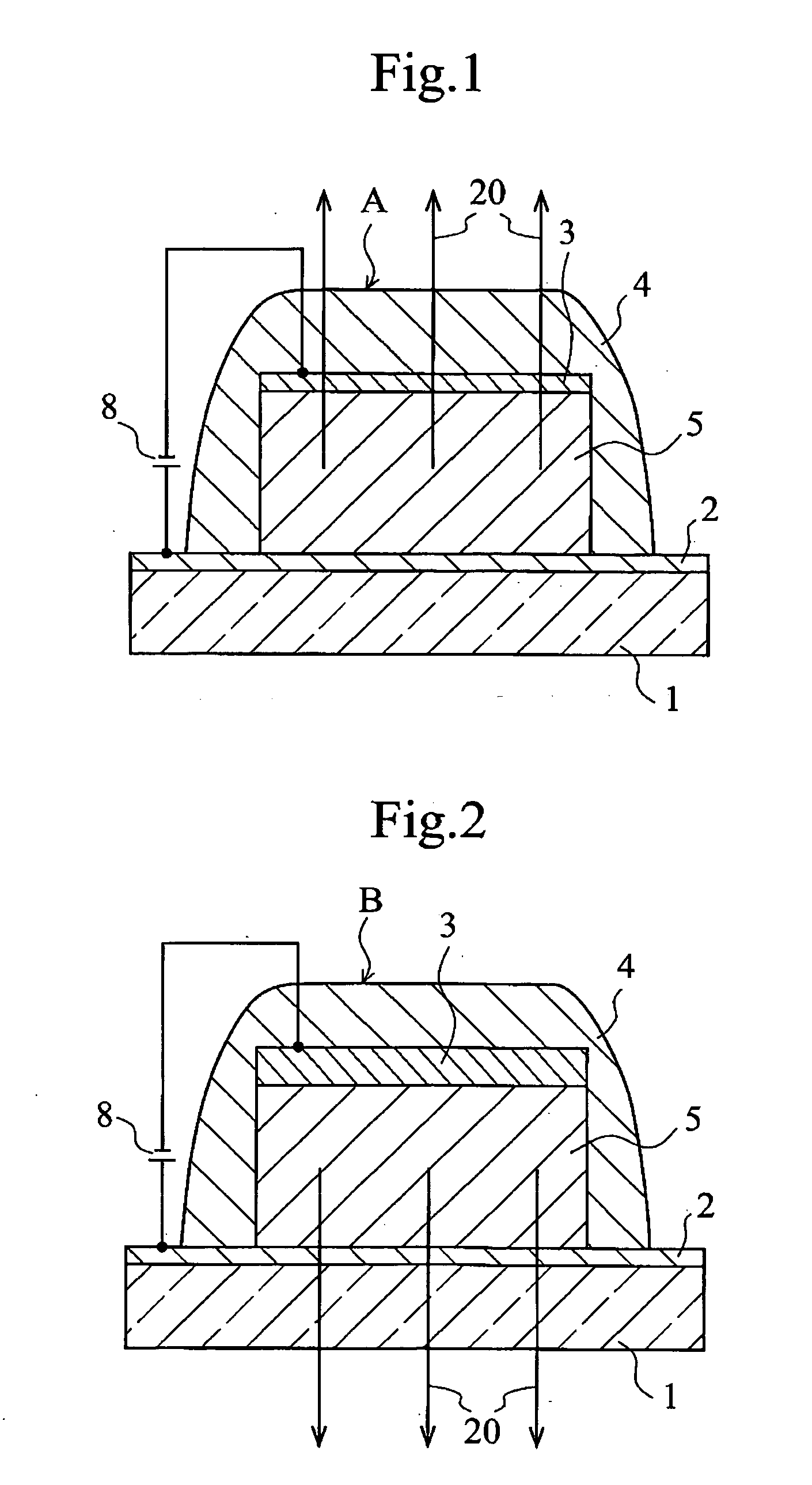
[0086] This example demonstrates an organic electroluminescent element (bottom emitting type) of single hetero structure in which the hole transporting layer which functions also as the emitting layer (hole transporting and emitting layer) is formed from a mixture of an aminostyryl compound represented by the structural formula (17)-11 below (which is one of the styryl compounds represented by the general formula [I] given above) and α-NPD (α-naphthylphenyldiamine).

[0087] First, a glass substrate, measuring 30 mm by 30 mm, was placed in a vacuum deposition apparatus. This glass substrate has an anode of ITO film (100 nm thick) formed on one surface thereof. The glass substrate underwent vacuum deposition at 10−4 Pa or less, with a metal mask arranged close thereto, which has a plurality of openings, each measuring 2.0 mm by 2.0 mm. The vacuum deposition gave rise to a 50-nm thick hole transporting layer (which functions also as the emitting layer) composed of the styryl compound r...

example 2

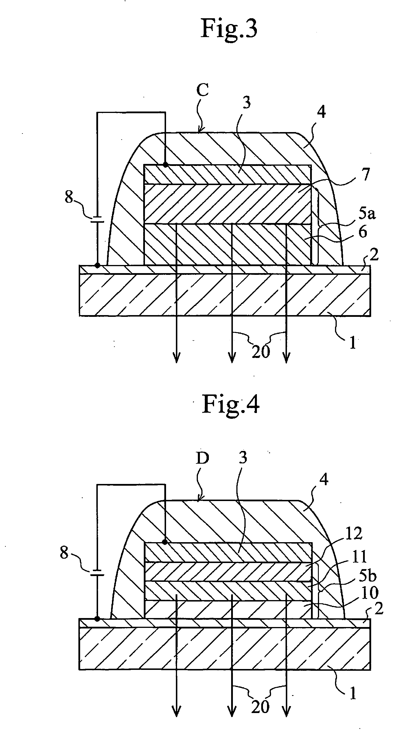
[0092] This example demonstrates an organic electroluminescent element (bottom emitting type) of single hetero structure in which the electron transporting layer which functions also as the emitting layer (electron transporting and emitting layer) is formed from a mixture of a styryl compound represented by the structural formula (17)-11 given above (which is one of the styryl compounds represented by the general formula [I] given above) and Alq3 represented by the structural formula given above.

[0093] First, a glass substrate, measuring 30 mm by 30 mm, was placed in a vacuum deposition apparatus. This glass substrate has an anode of ITO film (100 nm thick) formed on one surface thereof. The glass substrate underwent vacuum deposition at 10−4 Pa or less, with a metal mask arranged close thereto, which has a plurality of openings, each measuring 2.0 mm by 2.0 mm. The vacuum deposition gave rise to a 50-nm thick layer of α-NPD represented by the structural formula given above. The ra...

example 3

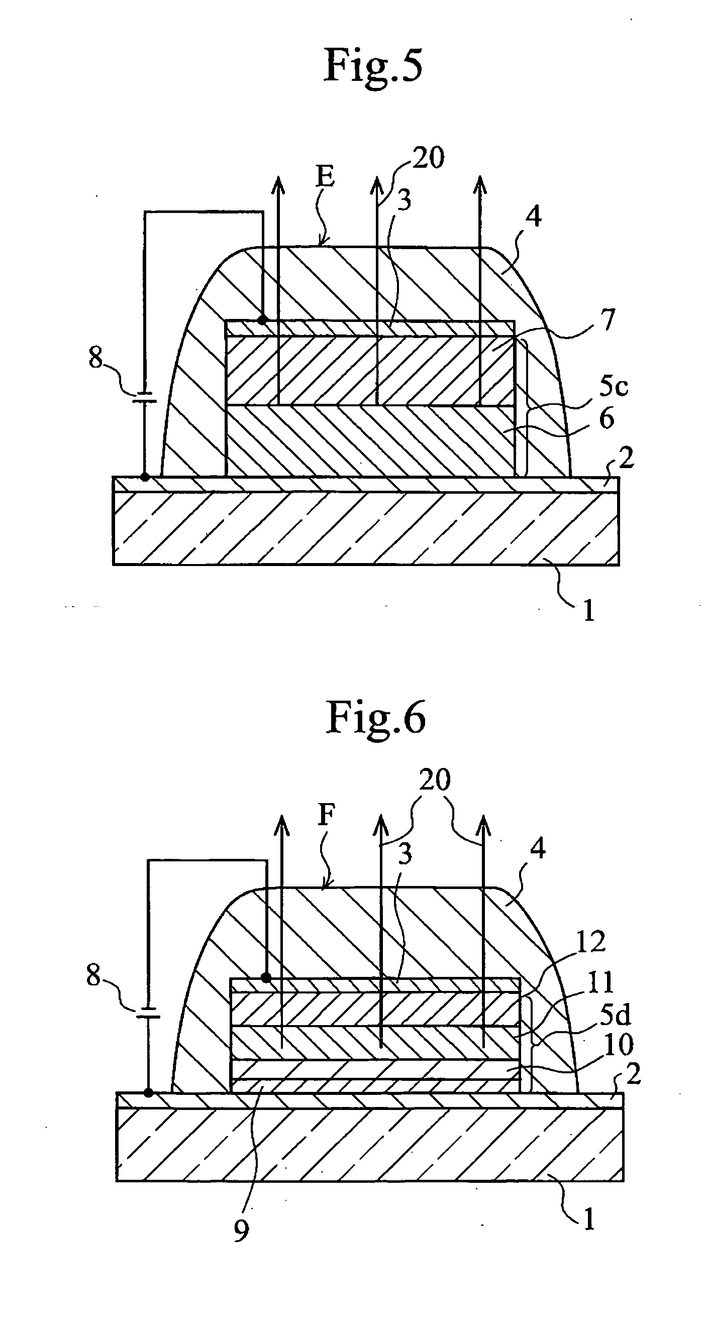
[0098] This example demonstrates an organic electroluminescent element (bottom emitting type) of double hetero structure in which the electron transporting and emitting layer is formed from a mixture of a styryl compound represented by the structural formula (17)-11 given above (which is one of the styryl compounds represented by the general formula [I] given above) and Alq3 represented by the structural formula given above.

[0099] First, a glass substrate, measuring 30 mm by 30 mm, was placed in a vacuum deposition apparatus. This glass substrate has an anode of ITO film (100 nm thick) formed on one surface thereof. The glass substrate underwent vacuum deposition at 10−4 Pa or less, with a metal mask arranged close thereto, which has a plurality of openings, each measuring 2.0 mm by 2.0 mm. The vacuum deposition gave rise to a 30-nm thick layer of α-NPD represented by the structural formula given above. The rate of deposition was adjusted to 0.2 nm / s.

[0100] Then, on the hole trans...


PUM

PropertyMeasurementUnit
Nanoscale particle sizeaaaaaaaaaa

Abstract

The present invention provides an organic electroluminescent element which is superior in luminance, reliability, and thermal stability and is capable of selectively emitting light with comparative long wavelengths such as red and good color purity and a light-emitting device or display device incorporated therewith. The organic electroluminescent element consists of a glass substrate (1), an anode (2), a hole transporting layer (10), an emitting layer (11), an electron transporting layer (12), and a cathode (3), which are sequentially laminated on top of the other. The emitting layer (11) is formed from a mixture composed of at least one species of the styryl compound represented by the general formula [I] below and a material with charge transporting capability.
Y—CH═CH—X   General formula [I]
(where X denotes an aryl group (such as phenyl group) which has a substituent group (such as cyano group and methyl group), and Y denotes a group having a skeleton of aminophenyl group or the like.)

Description

TECHNICAL FIELD [0001] The present invention relates to an organic electroluminescent element (organic EL element) having an organic layer for light emission which is sandwiched between the anode and the cathode, and also relates to a light-emitting device or display device incorporated therewith. BACKGROUND ART [0002] Enormous efforts are being directed to research and development of light-weight high-efficiency flat-panel displays for use as computer screens or television screens. [0003] One reason for this is that the conventional CRT now in general use as the display device is bulky, heavy, and power-consumptive despite its high luminance and good color reproduction. [0004] Among the light-weight high-efficiency flat-panel displays which have recently been commercialized is, for example, a liquid-crystal display of active matrix drive type. Unfortunately, it has a narrow viewing angle and needs back light (which consumes a large amount of electric power) for use in a dark place ...

Claims


Application Information

Patent Timeline
IPC IPC(8): C09K11/06H01L51/00H01L51/50H01L51/30
CPCC09K11/06C09K2211/1003C09K2211/1007C09K2211/1011C09K2211/1014C09K2211/1029Y10S428/917H01L51/0054H01L51/006H01L51/0081H01L51/5012H01L51/5048H01L51/0052H10K85/622H10K85/633H10K85/615H10K85/324H10K50/14H10K50/11
Inventor ISHIBASHI, TADASHIICHIMURA, MARITAMURA, SHINICHIROUEDA, NAOYUKI
Owner JOLED INC
Why Eureka
Try Eureka