Dual panel-type organic electroluminescent device and method for fabricating the same

Active Publication Date: 2005-07-28
LG DISPLAY CO LTD
View PDF15 Cites 61 Cited by
  • Summary
  • Abstract
  • Description
  • Claims
  • Application Information

AI Technical Summary

Benefits of technology

[0027] An object of the present invention is to provide an organic electroluminescent device having an improved production yield and reduced productions costs.
[

Problems solved by technology

Since they have a simple manufacturing processes, the degree of environmental contamination created by the manufacture of OELD devices is relatively low.
The production yield of the overall OELD device becomes limited by the organic EL diode's yield.
For example, even when a TFT is properly fabricated, the OELD device using a thin film of about 1000 angstroms (Å) thickness can be judged to be inferior due to defects in an organic electroluminescent layer.
This results in loss of materials and increased production costs.
However, the bottom emission-type OELD devices are ineffective as high resolution devices since the disposition of the thin film transistors and the storage capacitor formed on the substrate results in poor aperture ratios.
As a result, transmittance and optic

Method used


Image

  • Dual panel-type organic electroluminescent device and method for fabricating the same
  • Dual panel-type organic electroluminescent device and method for fabricating the same
  • Dual panel-type organic electroluminescent device and method for fabricating the same

Examples


Example

[0055] Reference will now be made in detail to the preferred embodiments of the present invention, examples of which are illustrated in the accompanying drawings.

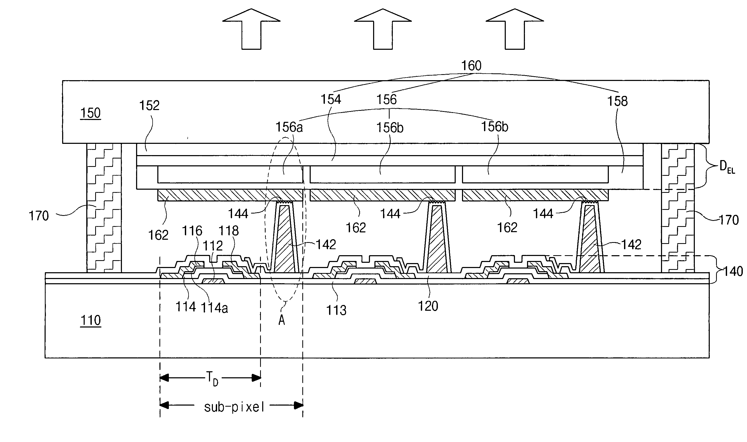
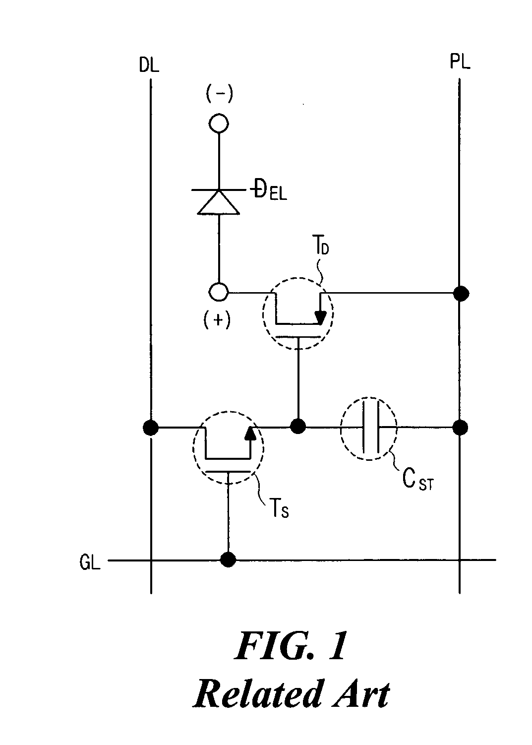
[0056]FIG. 6 is a cross-sectional view of an exemplary dual panel-type OELD device according to an embodiment of the present invention. As shown in FIG. 6, first and second spaced-apart substrates 110 and 150, which both include inner surfaces facing each other, have a plurality of sub-pixel regions. An array layer 140 including a driving thin film transistor (TFT) TD within each sub-pixel region can be formed on an inner surface of the first substrate 110. A connection pattern 142 is formed on the array layer 140. A connection electrode layer 144 covers the connection pattern 142 and is connected to the driving TFT TD. The connection pattern 142 and the connection electrode layer 144 are disposed within each sub-pixel region. The connection electrode layer 144 may include conductive material, such as a metallic material, ...


PUM


Abstract

A dual panel-type active matrix organic electroluminescent device includes: first and second substrates spaced apart from each other; a driving thin film transistor on an inner surface of the first substrate; a connection electrode layer connected to the driving thin film transistor and formed of a first conductive material having a first hardness; a first electrode on an inner surface of the second substrate; an organic electroluminescent layer on the first electrode; and a second electrode on the organic electroluminescent layer, the second electrode connected to the connection electrode layer and formed of a second conductive material having a second hardness, wherein the first hardness is different from the second hardness.

Description

[0001] The present invention claims the benefit of Korean Patent Application Nos. 2003-0091527 and 2003-0101282 filed in Korea on Dec. 15, 2003 and Dec. 31, 2003, respectively, which are hereby incorporated by reference. BACKGROUND OF THE INVENTION [0002] 1. Field of the Invention [0003] The present invention relates to an organic electroluminescent display device, and more particularly, to a dual panel-type organic electroluminescent display device. [0004] 2. Discussion of the Related Art [0005] As the need for information technology increases, the need for flat panel displays having thin profiles, lightweight, and lower power consumption also increases. Accordingly, various flat panel display (FPD) devices, such as liquid crystal display (LCD) devices, plasma display panel (PDP) devices, field emission display devices, and electro-luminescence display (ELD) devices, have been developed. ELD devices make use of an electro-luminescence phenomenon in which light is generated when an ...

Claims


Application Information

Patent Timeline
IPC IPC(8): H01L21/00H01L21/77H01L21/84H01L27/01H01L27/12H01L27/32H05B33/10H05B33/12H05B33/22H05B33/26H05B44/00
CPCH01L27/12H01L27/3253H01L27/1214H01L27/1255H01L29/41733H10K59/1275
Inventor PARK, JAE-YONGKIM, SUNG-KIKIM, HAE-YEOL
Owner LG DISPLAY CO LTD
Why Eureka
Try Eureka