Electrostatic discharge input and power clamp circuit for high cutoff frequency technology radio frequency (RF) applications

Inactive Publication Date: 2005-07-28
IBM CORP
View PDF2 Cites 20 Cited by
  • Summary
  • Abstract
  • Description
  • Claims
  • Application Information

AI Technical Summary

Benefits of technology

[0021] The present invention provides an ESD device network that is suitable for imple

Problems solved by technology

Electrostatic Discharge (ESD) events, which can occur both during and after manufacturing of an Integrated Circuit (IC), can cause substantial damage to the IC.
ESD events have become particularly troublesome for CMOS and BiCMOS chips because of their low power requirements and extreme sensitivity.
When a transistor is exposed to an ESD event, the charge applied may cause an extremely high current flow to occur within the device, which can, in turn cause permanen

Method used


Image

  • Electrostatic discharge input and power clamp circuit for high cutoff frequency technology radio frequency (RF) applications
  • Electrostatic discharge input and power clamp circuit for high cutoff frequency technology radio frequency (RF) applications
  • Electrostatic discharge input and power clamp circuit for high cutoff frequency technology radio frequency (RF) applications

Examples


Embodiment Construction

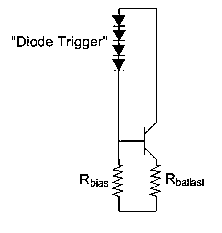
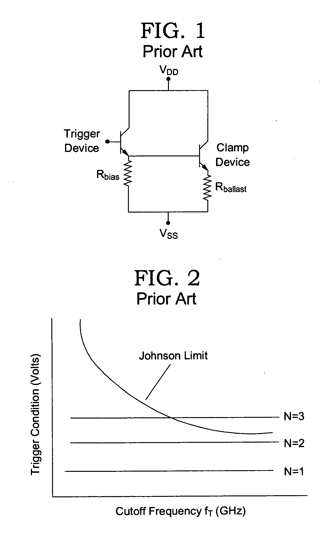
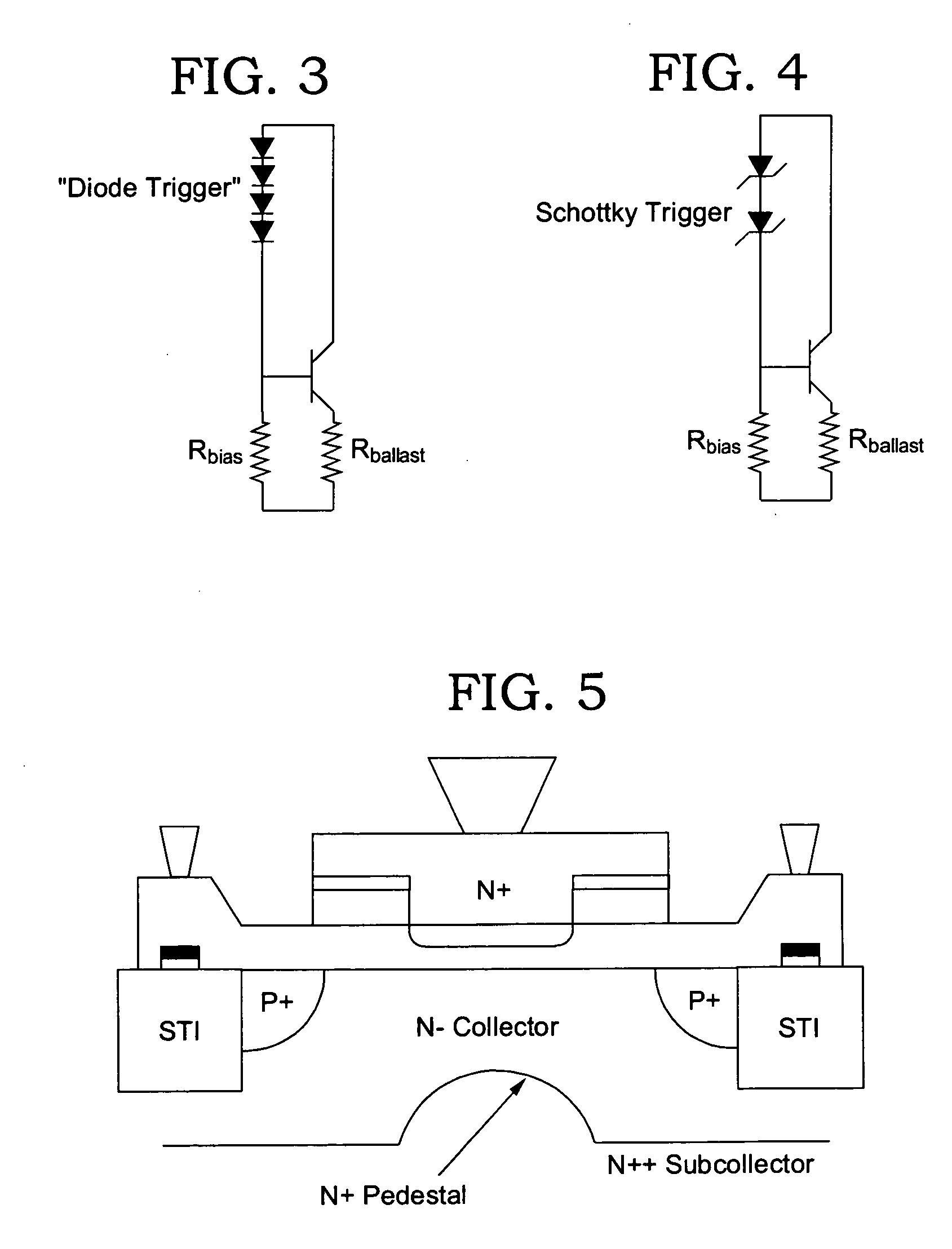
[0034]FIG. 1 illustrates an exemplary circuit of a prior art SiGe ESD power clamp wherein a first stage low breakdown transistor device serves as a trigger for a second stage high breakdown clamp transistor device. The first stage trigger transistor has a resistor Rbias in series therewith between power supplies VDD and VSS, and the second stage clamp transistor has a resistor Rballast in series therewith between the power supplies VDD and VSS. The circuit of FIG. 1 is a common emitter circuit with SiGe or SiGeC devices having floating bases, wherein the devices closely approximate the Johnson Limit curve.

[0035]FIG. 1 illustrates an exemplary Darlington configured bipolar power clamp circuit with a sub-native trigger voltage. For this configuration to be suitable as an ESD power clamp, we can take advantage of the inverse relationship between the BVCEO and the fT of the device. For a power clamp, the clamp device must have a high breakdown voltage in order to address the functional...


PUM


Abstract

A SiGe ESD (electrostatic discharge) power clamp circuit having a forward biased trigger device fabricated in a given technology and a clamp transistor preferably comprising a high frequency cutoff SiGe npn transistor, wherein the trigger device has a turn-on voltage which is below the Johnson Limit breakdown voltage of the highest frequency device fabricated in the given technology.

Description

BACKGROUND OF INVENTION [0001] 1. Field of the Invention [0002] The present invention relates generally to an electrostatic discharge input and power clamp circuit for high cutoff frequency technology radio frequency (RF) applications. [0003] More particularly, the subject invention relates to an electrostatic discharge input and power clamp circuit for high cutoff frequency technology RF applications with low voltage trigger elements and low power applications, and utilizing a forward biased junction trigger device and a low capacitance ESD NPN clamp transistor. [0004] 2. Discussion of the Prior Art [0005] The present invention relates generally to electrostatic discharge circuits, and more specifically pertains to electrostatic discharge power clamp circuits for high frequency RF applications. [0006] Electrostatic Discharge (ESD) events, which can occur both during and after manufacturing of an Integrated Circuit (IC), can cause substantial damage to the IC. ESD events have become...

Claims


Application Information

Patent Timeline
IPC IPC(8): H01L27/02H01L29/06H01L29/737
CPCH01L27/0259H01L29/0657H01L29/7378H01L2924/0002H01L2924/00
Inventor VOLDMAN, STEVEN H.
Owner IBM CORP
Why Eureka
Try Eureka