Micromirrors with support walls

a technology of micromirrors and support walls, which is applied in the field of micromirror arrays, can solve the problems of limiting the deflection of reflecting elements, and achieve the effects of reducing the reflective area of each micromirror, reducing the diffraction effect, and lowering the optical performance of the micromirror

Inactive Publication Date: 2005-07-28
ISHII FUSAO +1
View PDF14 Cites 20 Cited by
  • Summary
  • Abstract
  • Description
  • Claims
  • Application Information

AI Technical Summary

Benefits of technology

[0019] The present invention relates to micromirror devices and arrays of micromirror devices. Such arrays may be used as spatial light modulators (SLMs). In one aspect, the present invention provides a micromirror device in which the reflecting element is supported by a support structure comprising at least 1 wall. Said support structure is mechanically robust and lightweight. As a result, the micromirror device has superior mechanical properties. Another feature of support structures comprising support walls is that the orientation of the walls with respect to the incident light can be adjusted to reduce diffraction. Yet another feature of support structures comprising support walls is that the area of the portions of support structures that are exposed to incident light can be reduced or eliminated. As a result, the contrast ratio of the spatial light modulator (SLM) can be improved.
[0020] In another aspect, the present invention provides a micromirror device comprising a reflecting element, a support structure for said reflecting element comprising at least 1 support wall, and a deformable element. The support structure connects the reflecting element to the deformable element. The material for the deformable element is a polycrystalline or monocrystalline semiconductor. In a preferred embodiment, the deformable element is a torsion hinge. In a preferred embodiment, the semiconductor is silicon. The use of a polycrystalline or monocrystalline semiconductor as the material for the deformable element improves the fatigue strength of the deformable element. As a result, the reliability of the spatial light modulator (SLM) is improved.
[0021] In yet another aspect, the present invention provides a micromirror device comprising a reflecting element, a support structure for said reflecting element comprising at least 1 support wall, a deformable element, and support structures for said deformable element. Furthermore, the support structures for the deformable element limit the deflection of the reflecting element. This device structure simplifies the micromirror fabrication process while preventing the reflecting element from contacting the addressing electrodes.
[0029] In a preferred embodiment, the 3-layer substrate is a silicon-on-insulator (SOI) substrate, and the 3rd layer is the epitaxial silicon layer. In this case, the deformable element consists of epitaxial silicon, which is essentially monocrystalline silicon. An advantageous feature of this method is that monocrystalline silicon is used as the material for the deformable element. This improves the lifetime of the deformable element. In a preferred embodiment, addressing circuits and addressing electrodes are provided on the substrate during the aforementioned fabrication process. Circuits may be fabricated on the side of the substrate closer to the deformable elements or on the side farther away from the deformable elements or on both sides of the substrate. In a preferred embodiment, circuits may require Al or Al alloy metallization (e.g. CMOS circuits) and support structures for the deformable and reflecting elements are fabricated from polycrystalline silicon. Generally, the steps of depositing polysilicon are performed before the steps of Al or Al alloy metallization.

Problems solved by technology

Furthermore, the support structures for the deformable element limit the deflection of the reflecting element.

Method used


Image

  • Micromirrors with support walls
  • Micromirrors with support walls
  • Micromirrors with support walls

Examples


Embodiment Construction

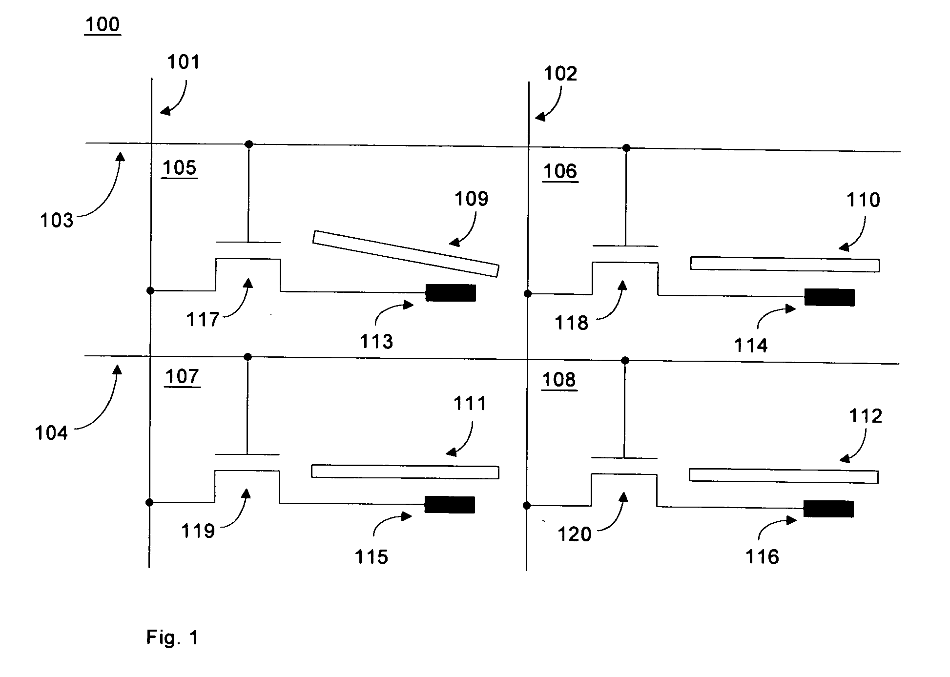
[0046] The present invention relates to electromechanical micromirror devices and arrays of such devices. Shown schematically in FIG. 1 is an array 100 comprising vertical data lines (101 and 102) and horizontal addressing lines (103 and 104), with each intersection of these data and addressing lines forming an electromechanical micromirror device (105, 106, 107, and 108). Each micromirror device comprises a micromirror (109, 110, 111, and 112), an addressing electrode (113, 114, 115, and 116), and an NMOS transistor (117, 118, 119, and 120). Micromirror 109 is shown to be in a deflected state while the other micromirrors are in their undeflected states. A possible scheme for addressing the micromirrors is as follows: The micromirrors (109, 110, 111, and 112) are electrically connected to ground. The deflection of a micromirror is determined by the bias voltage between the micromirror and its addressing electrode. The desired bias voltage is set by the voltages on the vertical data ...


PUM

PropertyMeasurementUnit
angleaaaaaaaaaa
angleaaaaaaaaaa
angleaaaaaaaaaa

Abstract

A micromirror device comprises a reflective element that is supported by at least 1 support wall. Support walls are designed for providing devices with improved mechanical and optical performance. Support walls are supported by a deformable element. The deformable element may be a torsion hinge. The deformable element may be supported by support structures that are designed to limit the deflection of the reflective element. An array of micromirror devices may be used as a spatial light modulator (SLM). Methods of fabricating micromirror arrays comprise the steps of: 1) providing a three-layer substrate, comprising a crystalline layer, a sacrificial layer, and a base layer, with the sacrificial layer being disposed between the crystalline layer and the base layer; 2) forming a deformable element in the crystalline layer; 3) forming support structures for the deformable element; and 4) forming electronic circuits on the base layer.

Description

TECHNICAL FIELD [0001] This invention relates to micromirror arrays and methods of manufacturing the same. Such arrays have applications in spatial light modulators (SLMs). BACKGROUND ART [0002] Electromechanical micromirror devices have drawn considerable interest because of their application as spatial light modulators (SLMs). A spatial light modulator requires an array of a relatively large number of such micromirror devices. In general, the number of devices required ranges from 60,000 to several million for each SLM. Despite significant advances that have been made in recent years, there is still a need for improvement in the performance and manufacturing yields of electromechanical micromirror devices. [0003] U.S. Pat. No. 4,956,619 discloses a prior art micromirror device. In U.S. Pat. No. 4,956,619, the hinge (deflectable element) is formed in the reflecting layer. A problem with this structure is that the hinge has surfaces and edges that cause diffraction of incident light...

Claims


Application Information

Patent Timeline
Patent Type & Authority Applications(United States)
IPC IPC(8): G02B26/08G02F1/03G02F1/07
CPCG02B26/0841
Inventor ISHII, FUSAOHIDE, FUMITOMO
Owner ISHII FUSAO
Why Eureka
Try Eureka