

Semiconductor device
- Summary
- Abstract
- Description
- Claims
- Application Information
AI Technical Summary
Benefits of technology
Problems solved by technology
Method used
Image

Examples
first preferred embodiment
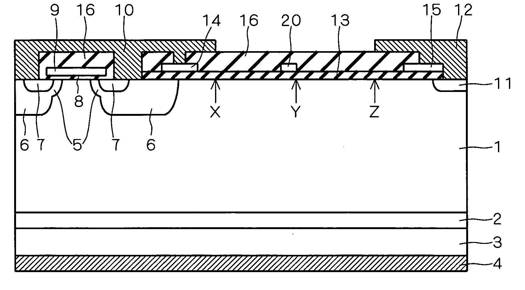
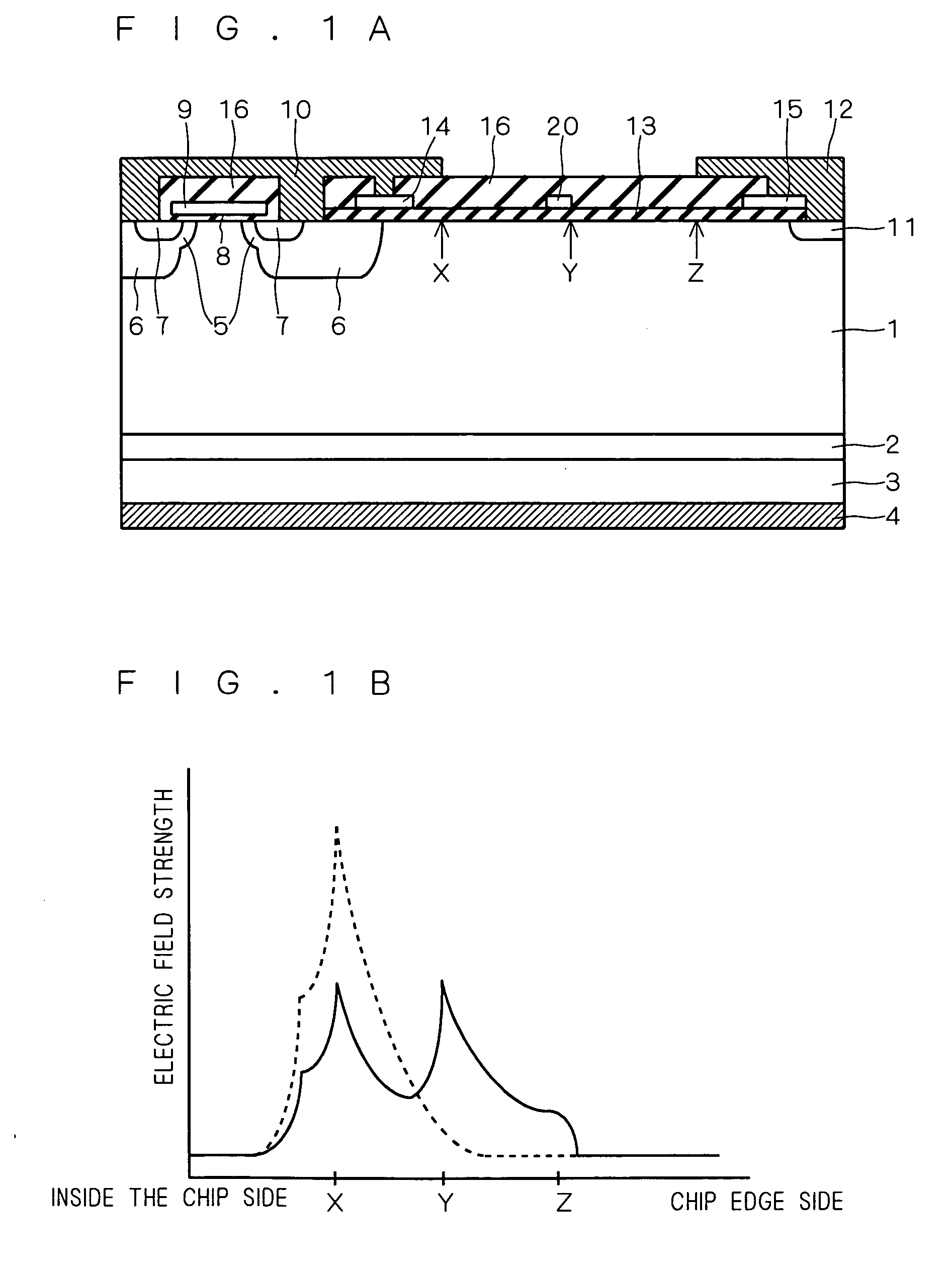
[0042]FIG. 1A illustrates the configuration of a semiconductor device according to a first preferred embodiment of this invention, which is a peripheral portion of a vertical IGBT chip. The left side portion of FIG. 1A is a region where an IGBT is formed as a semiconductor element for performing current switching, a cell portion of the IGBT. This portion is configured in a similar fashion as a typical IGBT. That is, on the under surface side of an n− drift layer 1, a p+ collector region 3 is formed via an n+ buffer layer 2 having lower resistance than the n− drift layer 1. A collector electrode 4 is provided on the under surface of the p+ collector region 3. In a surface layer on the top surface side of the n− drift layer 1, a p base region 5 is formed and, in order to prevent latchup of a parasitic thyristor, a p+ isolation well 6 is formed to overlap part of the p base region 5, the p+ isolation well 6 being of higher concentration and diffused deeper than the p base region 5. An ...
second preferred embodiment
[0060]FIG. 5 illustrates the configuration of a semiconductor device according to a second preferred embodiment of this invention, which is different from that shown in FIG. 1A in that a gate wiring 19 is connected to the field plate 14 on the low voltage side. Although not shown, the gate wiring 19 is electrically connected to the gate electrode 9. Namely, the field plate 14 and the gate electrode 9 are equal in potential. In FIG. 5, elements identical to those in FIG. 1A are denoted by like reference numbers, and descriptions thereof will thus be omitted. In this example, the outermost electrode (second electrode) on the substrate in the IGBT cell is the gate wiring 19.
[0061] Again in the FIG. 5 semiconductor device, there is provided the intermediate potential electrode 20 between the field plates 14 and 15 on the field oxide film 13. The electrode 20 is supplied with a lower intermediate potential than the silicon substrate surface therebelow from the intermediate potential app...
third preferred embodiment
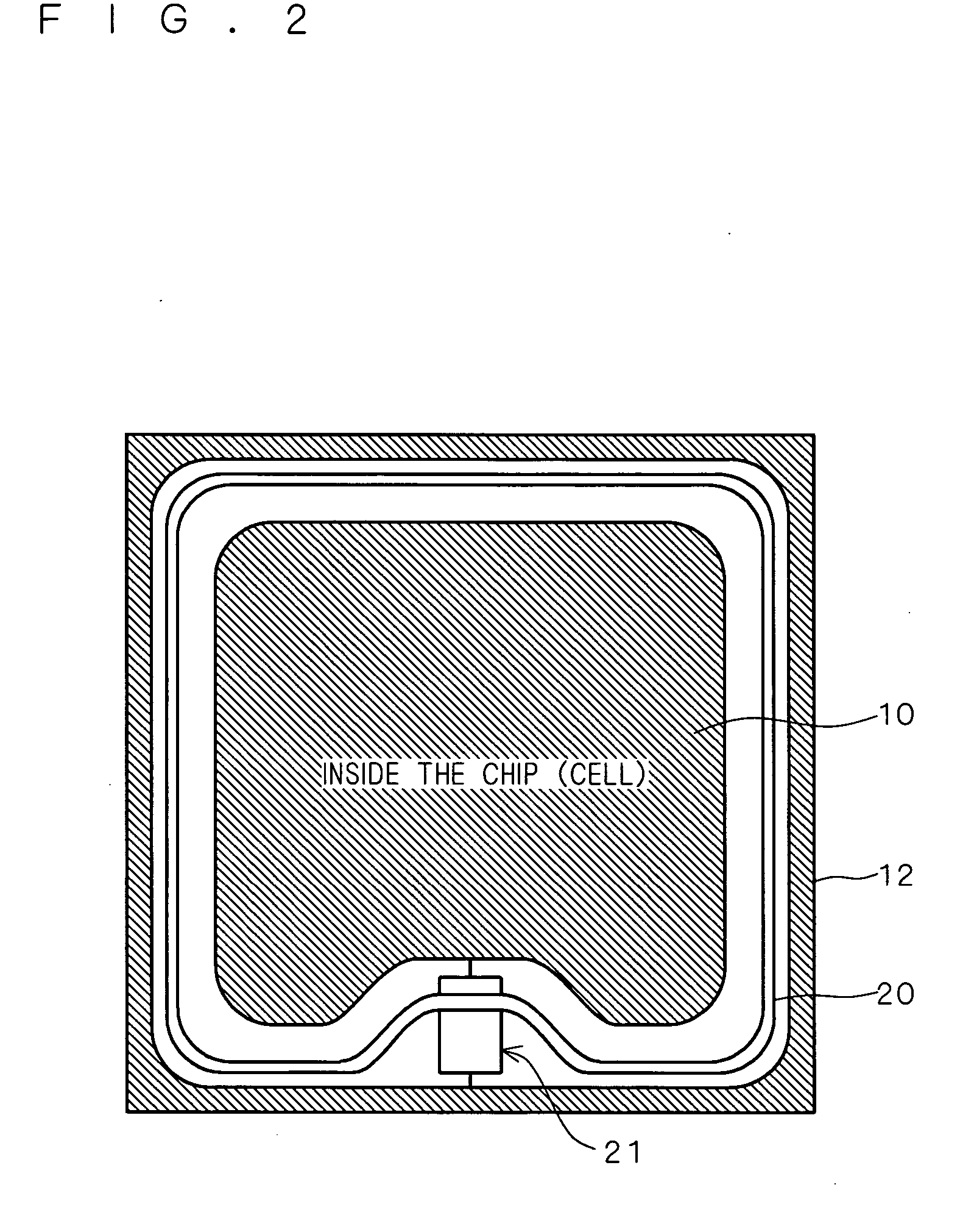
[0072] In a third preferred embodiment of this invention, a plurality of intermediate potential electrodes are provided on the chip peripheral portion. For instance, FIG. 9A illustrates the semiconductor device according to the first preferred embodiment including two intermediate potential electrodes 20a and 20b. The other components in FIG. 9A are identical to those in FIG. 1A, and detailed descriptions of FIG. 9A will thus be omitted.
[0073] When, with the potential at the collector electrode 4 (potential at the channel stopper electrode 12) being higher than the emitter electrode 10, the electrodes 20a and 20b are set to have a lower potential than the silicon substrate surface therebelow, a depletion layer extends easily in the n− drift layer 1 in the chip peripheral portion below the respective electrodes 20a and 20b. Conversely, when the electrodes 20a and 20b are set to have a higher potential than the silicon substrate surface therebelow, extension of a depletion layer is s...
PUM
 Abstract
Description
Claims
Application Information