Light-emitting semiconductor device with a built-in overvoltage protector

Active Publication Date: 2005-08-04
SANKEN ELECTRIC CO LTD
View PDF1 Cites 62 Cited by
  • Summary
  • Abstract
  • Description
  • Claims
  • Application Information

AI Technical Summary

Benefits of technology

[0006] The present invention seeks to make an integrated combination of a light-emitting diode and an overvoltage protector simpler in constr

Problems solved by technology

The nitride semiconductor light-emitting devices have, however, an inherent weakness in withstanding electrostatic breakdown, being susceptible to destruction when subjected to a voltage surge in excess of 100 volts.
This remedy is unsatisfactory in consideration of the bulk of the resulting device caused factory in consideration of the bulk of the resulting device caused by the added number of component parts.
The suggestions made by these unexa

Method used


Image

  • Light-emitting semiconductor device with a built-in overvoltage protector
  • Light-emitting semiconductor device with a built-in overvoltage protector
  • Light-emitting semiconductor device with a built-in overvoltage protector

Examples


embodiment

of FIG. 5

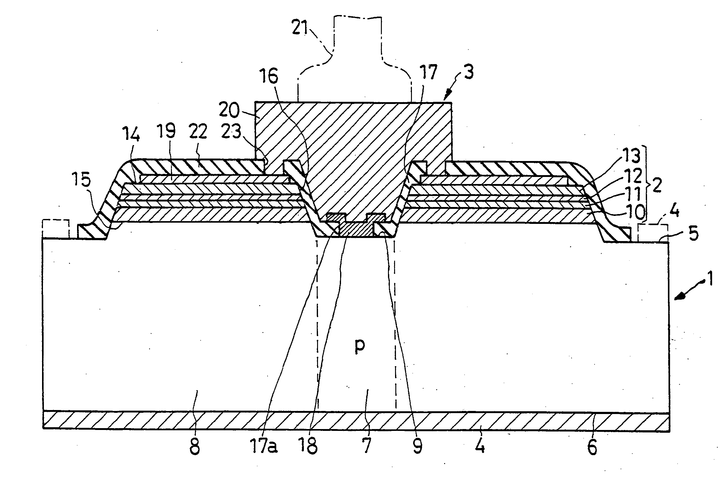
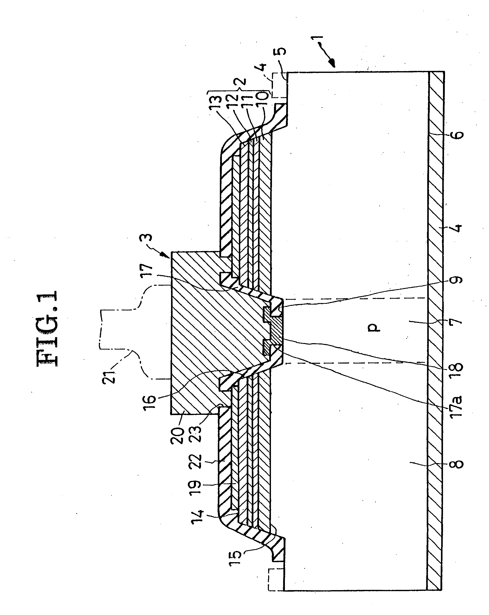
[0062] Another preferred form of overvoltage-proof LED shown in FIG. 5 features a pn-junction diode employed as an overvoltage protector in lieu of the Schottky barrier diode of the preceding embodiment. An n-type semiconductor region 40 is formed in part of the protector region 7 of the silicon semiconductor substrate 1 in order to provide the pn-junction diode. This embodiment also differs from that of FIGS. 1-4 in having no metal region 18 seen in FIG. 1.

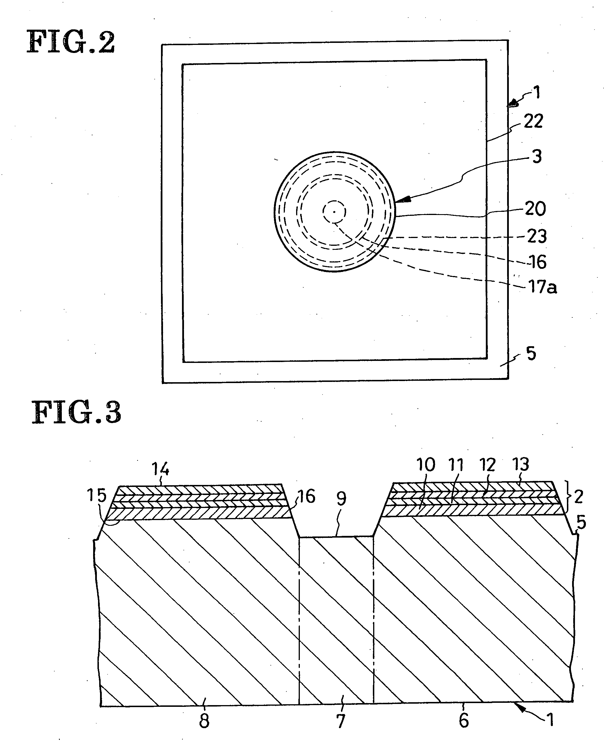
[0063] The pn-junction protector diode is comprised of the noted n-type semiconductor region 40 which is formed island-like in the protector region 7 of the substrate 1 so as to be exposed at the major surface 5 of the substrate, and the remaining p-type part of the substrate. The n-type region 40 is formed by diffusing an n-type impurity into part of the preformed p-type substrate 1. It will be seen that the n-type region 40 is exposed at the bottom of the depression 9 formed in the surface of the protector region 7. T...


PUM


Abstract

An overvoltage-proof light-emitting diode has a lamination of light-generating semiconductor layers on a first major surface of a silicon substrate. A front electrode in the form of a bonding pad is mounted centrally atop the light-generating semiconductor layers whereas a back electrode covers a second major surface of the substrate. An overvoltage protector, of which several different forms are disclosed, is disposed between the bonding pad and the second major surface of the substrate. The bonding pad and back electrode serves as electrodes for both LED and overvoltage protector. As seen from above the device, or in a direction normal to the first major surface of the substrate, the overvoltage protector lies substantially wholly beneath the bonding pad.

Description

CROSS REFERNCE TO RELATED APPLICATIONS [0001] This application claims priority to Japanese Patent Application No. 2004-026102, filed Feb. 2, 2004, and Japanese Patent Application No. 2004-217715, filed Jul. 26, 2004. BACKGROUND OF THE INVENTION [0002] This invention relates to a light-emitting semiconductor device such as that known as a light-emitting diode in common parlance, and more specifically to such a device fabricated in one piece with an overvoltage protector. [0003] A host of specialists in light-emitting diodes have focused their attention in recent years on nitride semiconductors. The devices built using these materials emit light in the wavelength range of from 365 to 550 nanometers. The nitride semiconductor light-emitting devices have, however, an inherent weakness in withstanding electrostatic breakdown, being susceptible to destruction when subjected to a voltage surge in excess of 100 volts. It might be contemplated to incorporate an overvoltage or surge protector...

Claims


Application Information

Patent Timeline
IPC IPC(8): H01L27/15H01L33/38H02H9/00
CPCH01L27/15H01L2924/3025H01L24/05H01L2224/05555H01L2224/45124H01L2224/45144H01L2224/48463H01L33/385H01L2224/04042H01L2924/3011H01L2924/12032H01L2924/00014H01L2924/00H01L2924/12035H01L2924/12036H01L2924/12041
Inventor SATO, JUNJIOTSUKA, KOJIMOKU, TETSUJIKATO, TAKASHINIWA, AREIKAMII, YASUHIRO
Owner SANKEN ELECTRIC CO LTD
Why Eureka
Try Eureka