P-type zinc oxide semiconductor film and process for preparation thereof

a technology of zinc oxide and semiconductor film, applied in the direction of conductors, non-metal conductors, condensed vapors, etc., can solve the problem of rendering them insulativ

Inactive Publication Date: 2005-08-04
SANYO ELECTRIC CO LTD
View PDF7 Cites 39 Cited by
  • Summary
  • Abstract
  • Description
  • Claims
  • Application Information

AI Technical Summary

Benefits of technology

[0011] Also, a larger proportion of the donor defects which impede p-type conduction of the ZnO film is concentrated toward both ends in a thickness direction of the ZnO film. Therefore, if an alkali metal, e.g., lithium, is contained such that a concentration thereof is distributed to increase toward a surface of the film and/or toward an interface between the film and ...

Problems solved by technology

In ZnO semiconductor films, mere doping of nitrogen does not enable the p-type conduction thereof but causes self-c...

Method used


Image

  • P-type zinc oxide semiconductor film and process for preparation thereof
  • P-type zinc oxide semiconductor film and process for preparation thereof
  • P-type zinc oxide semiconductor film and process for preparation thereof

Examples


example 1

[0029] Using the apparatus shown in FIG. 5, a ZnO semiconductor film doped with lithium and nitrogen was formed on a c-plane sapphire substrate. Referring to FIG. 5, a vacuum chamber 1 houses a substrate 3 held on a substrate holder 4 and a target 2 located to oppose to the substrate 3. A laser 11 emits a laser beam 7 which is reflected at a sequence of lenses 9 and 10, passes through a focusing lens 8 and then enters the vacuum chamber 1 where the target 2 is illuminated at its surface. A plume 6 is produced on the surface of the target 2 illuminated with the laser beam 7. Although not shown in FIG. 5, N (nitrogen) radicals 5 from an N radical source are introduced into the vacuum chamber 1.

[0030] Using the apparatus shown in FIG. 5, a p-type ZnO semiconductor film was formed under the following forming condition 1. The formed p-type ZnO semiconductor film was about 400 nm thick.

[0031] (Forming Condition 1) [0032] Forming method: PLD (pulsed laser deposition) method [0033] Target...

example 2

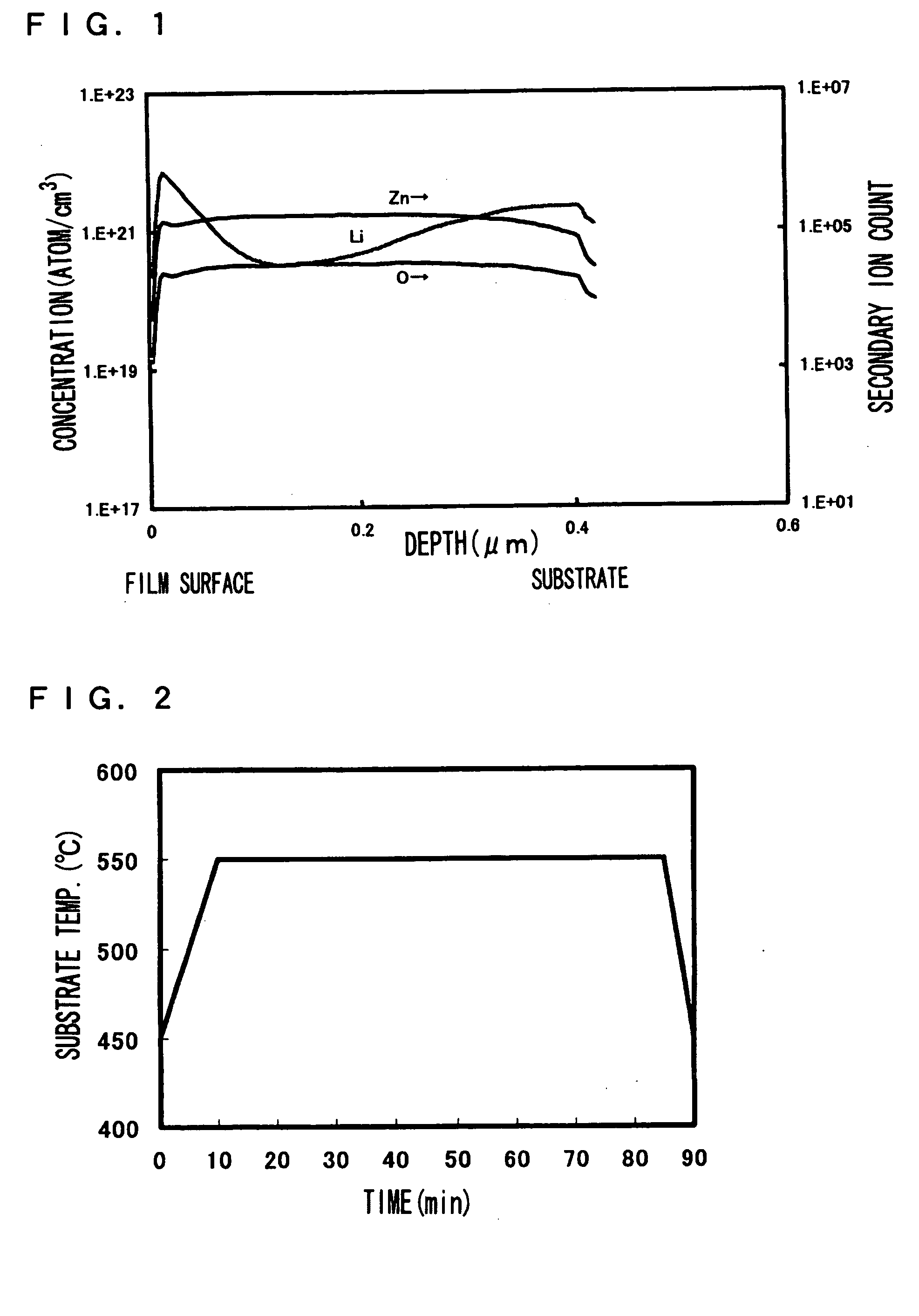
[0061] As shown in FIG. 2, the substrate temperature was controlled at relatively lower levels during the initial and final stages of film formation. Otherwise, The procedure of the preceding Example 1 was followed to form a ZnO film.

[0062] The resulting p-type ZnO film had a carrier concentration of 4×1016 cm−3 and showed a further property improvement over that obtained in Example 1.

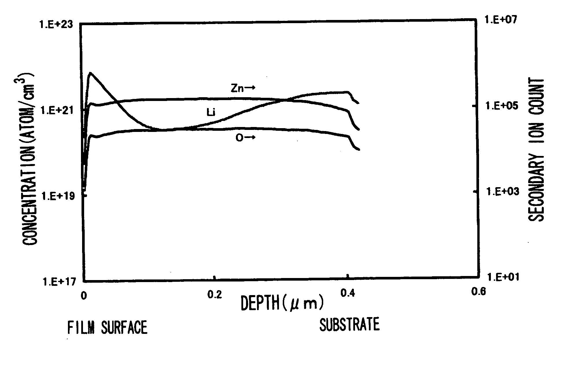
[0063]FIG. 1 is a graph showing an Li concentration profile in the thin film, when measured by SIMS. As shown in FIG. 1, the lithium content in the thin film is higher at locations closer to the film surface and the substrate surface. This is believed due to the substrate temperature that is controlled at lower levels during the initial and final stages of thin-film formation. The reason for the improvement in film properties when the lithium content is rendered higher at locations closer to the film surface and the substrate surface is most probably because a larger proportion of donor defects which...

example 3

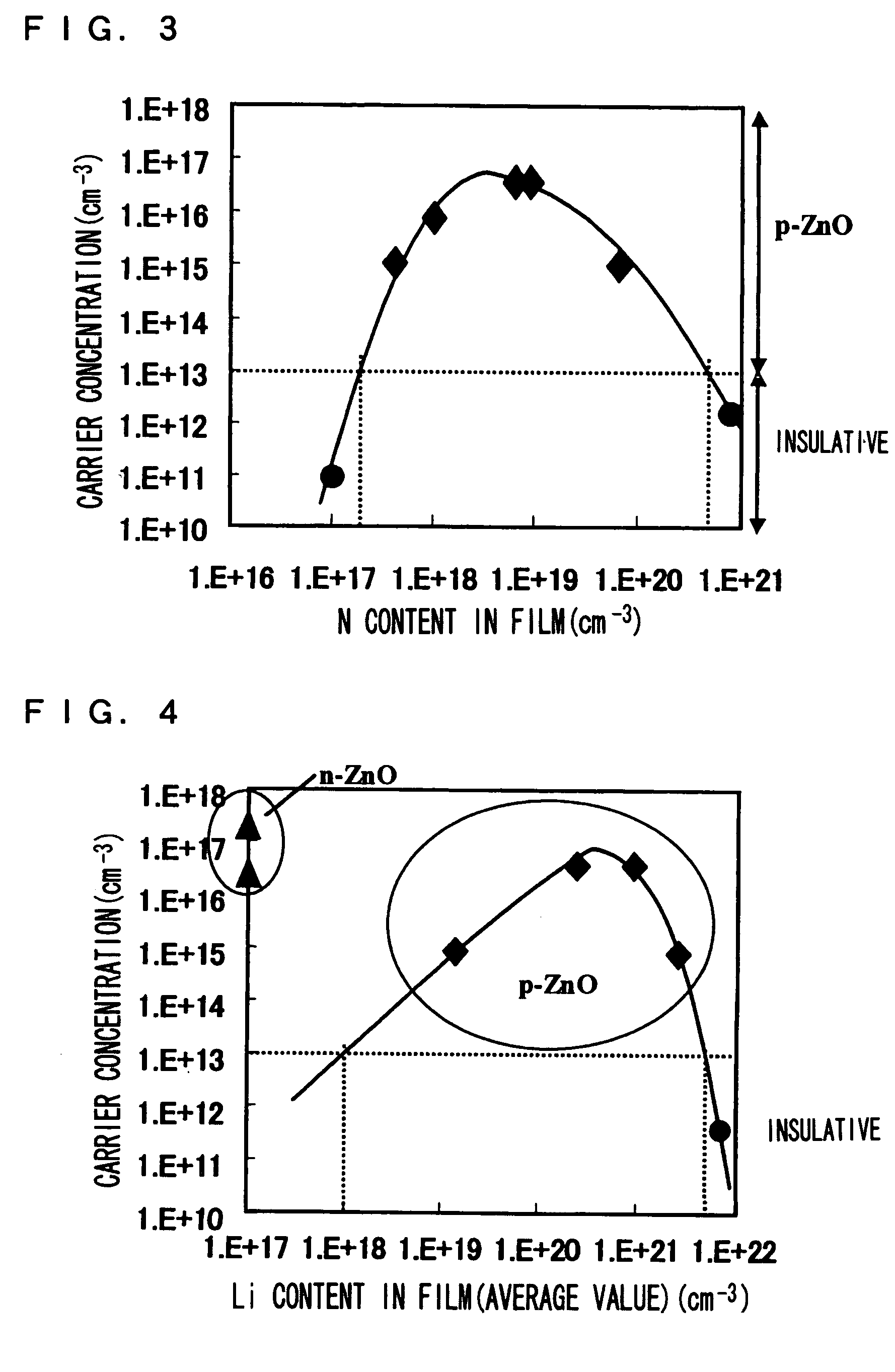
[0065] The influence of the carrier concentration on film properties was studied by varying a nitrogen content (amount of N) in a p-type ZnO semiconductor film.

[0066] The below-specified forming condition 4 was utilized to form a thin film. The nitrogen content in the thin film was varied by controlling an N radical source RF power and a substrate temperature. The nitrogen content in the film tends to increase with the higher N radical source RF power and decrease with the higher substrate temperature.

[0067] (Forming Condition 4) [0068] Forming method: PLD method [0069] Target: Li-doped ZnO target (Li content: 5 weight %) [0070] Laser: ArF laser [0071] Laser power: 1 J / cm2 [0072] Substrate temperature: 400-650° C. [0073] Chamber pressure: 3×10⁻² Pa [0074] N2 gas flow rate: 5 sccm [0075] N radical source RF power: 50-500 W [0076] (wherein the substrate temperature, while given above by the maximum value shown in FIG. 2, is controlled at a level 100° C. lower than the maximum level ...


PUM

PropertyMeasurementUnit
Carrier concentrationaaaaaaaaaa
Temperatureaaaaaaaaaa

Abstract

A p-type ZnO semiconductor film comprised mainly of Zn and O elements is disclosed. The film is characterized as containing an alkali metal and nitrogen. Preferably, the alkali metal is contained such that its concentration is distributed to increase toward an end or toward both ends in the thickness direction of the film. More preferably, the alkali metal is contained in the concentration range of 1×10¹⁸-5×1021 cm−3 and the nitrogen in the concentration range of 2×10¹⁷-5×1020 cm−3.

Description

[0001] The priority Japanese Patent Application Number 2004-20022 upon which this patent application is based is hereby incorporated by reference. BACKGROUND OF THE INVENTION [0002] 1. Field of the Invention [0003] The present invention relates to a p-type ZnO semiconductor film and a process for preparation thereof. [0004] 2. Description of Related Art [0005] In order to realize the new generation of electronic devices, e.g., transparent electronic circuits and ultraviolet light-emitting diodes, using oxide semiconductors, it is essential to develop p-type oxide semiconductors. Zinc oxide (ZnO), because of its high potential, has been recently noted as a promising material for such p-type oxide semiconductors and the associated research and development have been actively conducted. [0006] However, it is extremely difficult to prepare p-type ZnO and only a very few successful examples are reported. As a representative of such successful examples, a codoping method is known which inv...

Claims


Application Information

Patent Timeline
IPC IPC(8): C23C14/28C23C14/08H01B1/00H01L21/363
CPCC23C14/086C23C14/28H01L21/02631H01L21/02554H01L21/02579H01L21/0242
Inventor YATA, SHIGEOWAKISAKA, KENICHIROKOBAYASHI, TAKESHI
Owner SANYO ELECTRIC CO LTD
Why Eureka
Try Eureka