Nitride heterojunction transistors having charge-transfer induced energy barriers and methods of fabricating the same

a heterojunction transistor and charge-transfer technology, applied in the field of high-frequency transistors, can solve the problems of less common semiconductor materials that are not well suited for higher power and/or high frequency applications, the material quality in the layer begins to degrade, and the reliability of the device decreases

Active Publication Date: 2005-08-11
CREE INC
View PDF66 Cites 168 Cited by
  • Summary
  • Abstract
  • Description
  • Claims
  • Application Information

AI Technical Summary

Benefits of technology

[0023] The problems associated with free carrier trapping may also affect the performance of other types of nitride field effect transistors, such as GaN-based MESFETs.
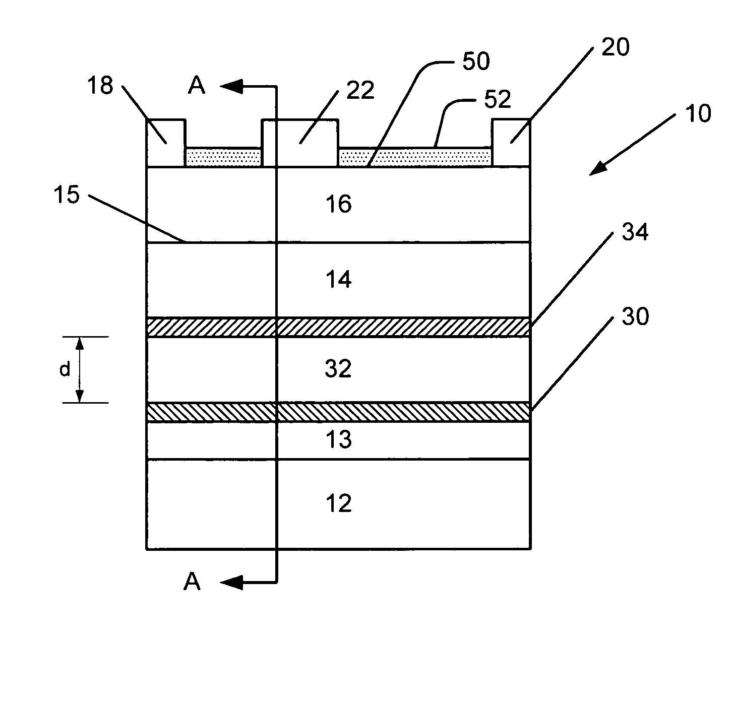
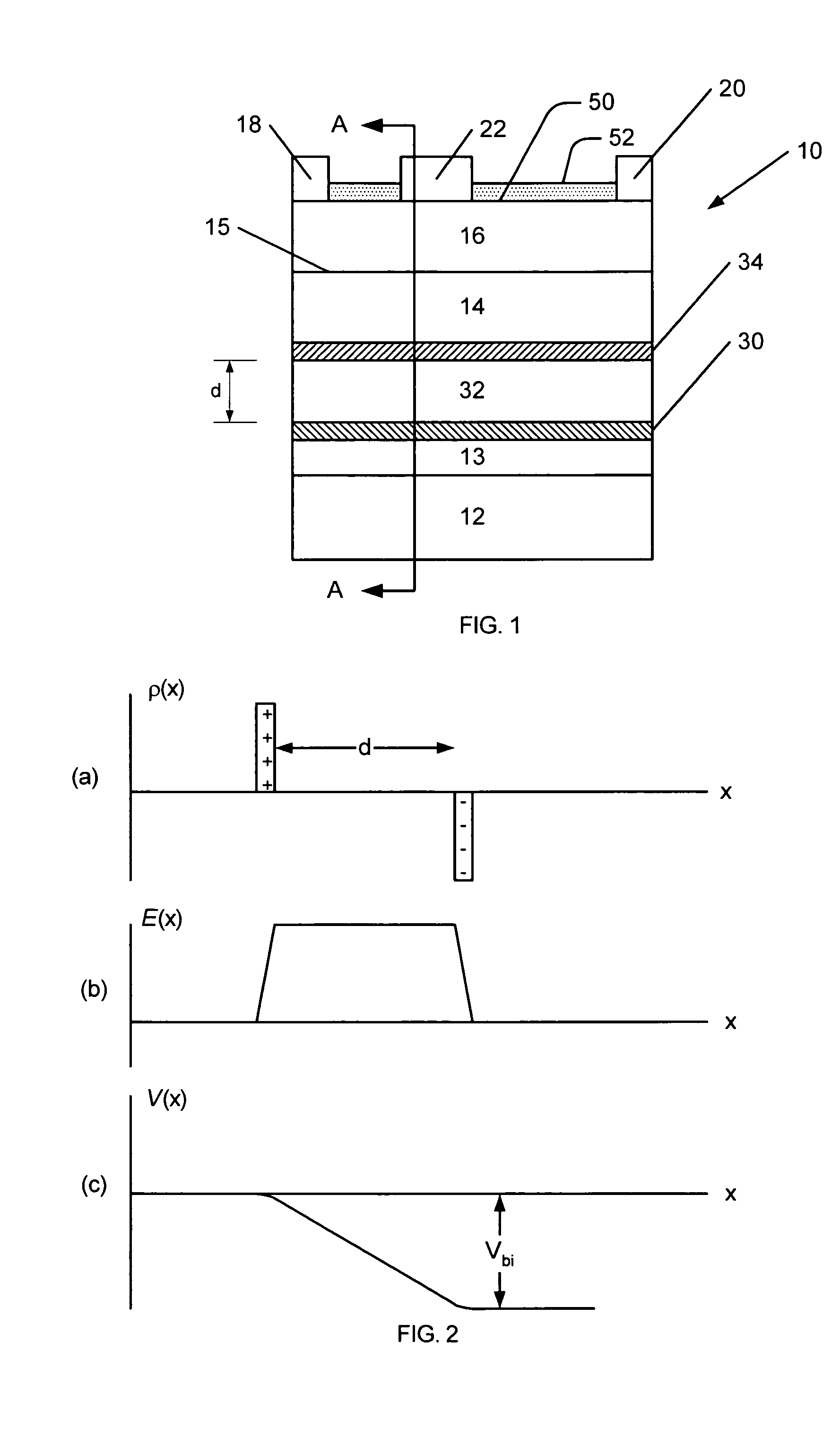
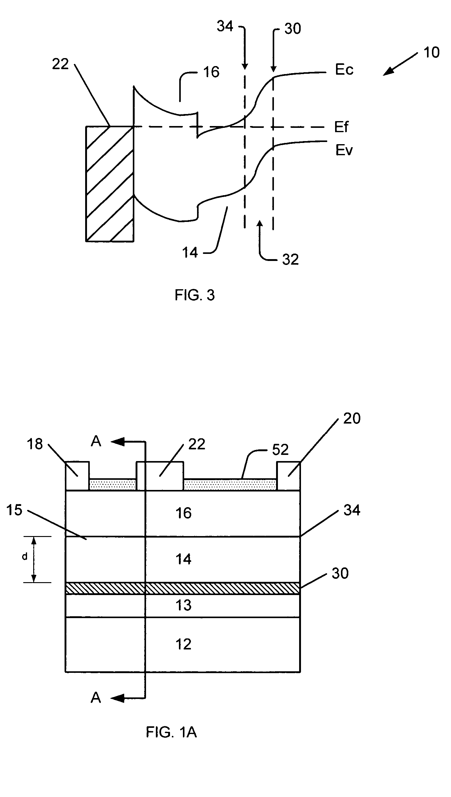
[0024] Embodiments of the present invention provide nitride-based field effect transistors having a substrate, a channel layer that includes InAlGaN formed on the substrate; source and drain ohmic contacts in electrical communication with the channel layer; and a gate contact formed on the channel layer. At least one energy barri

Problems solved by technology

These more common semiconductor materials may not be well suited for higher power and/or high frequency applications, however, because of their relatively small bandgaps (e.g., 1.12 eV for Si and 1.42 for GaAs at room temperature) and/or relatively small breakdown voltages.
However, GaAs has a relatively small bandgap (1.42 eV at room temperature) and relatively small breakdown voltage, which may prevent GaAs based HEMTs from providing high power at high frequencies.
Moreover, because the sheet charge region is extremely thin, the carriers are subject to reduced impurity scattering that may improve the device's noise characteristics.
However, the high lattice mismatch between AlN and GaN dictates that the thickness of the AlN layer should be less than 50 Å. If the layer is thicker, the device can experience problems with its ohmic contacts, the material quality in the layer begins to degrade, the device's reliability decreases, and the material is more difficult to grow.
However, a HEMT with a 50 Å or less AlN layer may be susceptible to high gate leakage.
Although GaN-based HEMTs have demonstrated exceptional power densities, a number of technical challenges still remain to be overcome before the devices can achieve commercial success.
For example, one problem that may limit the performance and lifetime of certain GaN-based HEMTs is free carrier trapping, w

Method used


Image

  • Nitride heterojunction transistors having charge-transfer induced energy barriers and methods of fabricating the same
  • Nitride heterojunction transistors having charge-transfer induced energy barriers and methods of fabricating the same
  • Nitride heterojunction transistors having charge-transfer induced energy barriers and methods of fabricating the same

Examples


Embodiment Construction

[0054] The present invention will now be described more fully with reference to the accompanying drawings in which some embodiments of the invention are shown. This invention may, however, be embodied in many different forms and should not be construed as limited to the embodiments set forth herein. Rather, these embodiments are provided so that this disclosure will be thorough and complete, and will fully convey the scope of the invention to those skilled in the art. Like numbers refer to like elements throughout.

[0055] Furthermore, the various layers and regions illustrated in the figures are illustrated schematically. Accordingly, the present invention is not limited to the relative size and spacing illustrated in the accompanying figures. As will also be appreciated by those of skill in the art, references herein to a layer formed “on” a substrate or other layer may refer to the layer formed directly on the substrate or other layer or on an intervening layer or layers formed on...


PUM


Abstract

A nitride-based field effect transistor includes a substrate, a channel layer comprising InAlGaN formed on the substrate, source and drain ohmic contacts in electrical communication with the channel layer, and a gate contact formed on the channel layer. At least one energy barrier opposes movement of carriers away from the channel layer. The energy barrier may comprise an electron source layer in proximity with a hole source layer which generate an associated electric field directed away from the channel. An energy barrier according to some embodiments may provide a built-in potential barrier in excess of about 0.5 eV. Method embodiments are also disclosed.

Description

BACKGROUND OF THE INVENTION [0001] 1. Field of the Invention [0002] The present invention relates to high frequency transistors and in particular relates to microwave field effect transistors (FETs) that incorporate nitride-based active layers. [0003] 2. Description of the Related Art [0004] The present invention relates to transistors formed of nitride semiconductor materials that can make them suitable for high power, high temperature, and / or high frequency applications. Materials such as silicon (Si) and gallium arsenide (GaAs) have found wide application in semiconductor devices for lower power and (in the case of Si) lower frequency applications. These more common semiconductor materials may not be well suited for higher power and / or high frequency applications, however, because of their relatively small bandgaps (e.g., 1.12 eV for Si and 1.42 for GaAs at room temperature) and / or relatively small breakdown voltages. [0005] GaAs based HEMTs have become the standard for signal am...

Claims


Application Information

Patent Timeline
IPC IPC(8): H01L21/335H01L29/20H01L29/207H01L29/778H01L29/80
CPCH01L29/2003H01L29/207H01L29/802H01L29/7783H01L29/66462
Inventor SAXLER, ADAM WILLIAM
Owner CREE INC
Why Eureka
Try Eureka