

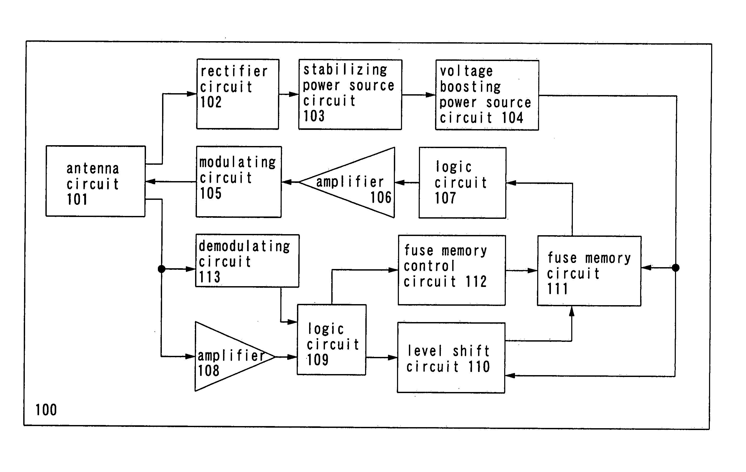
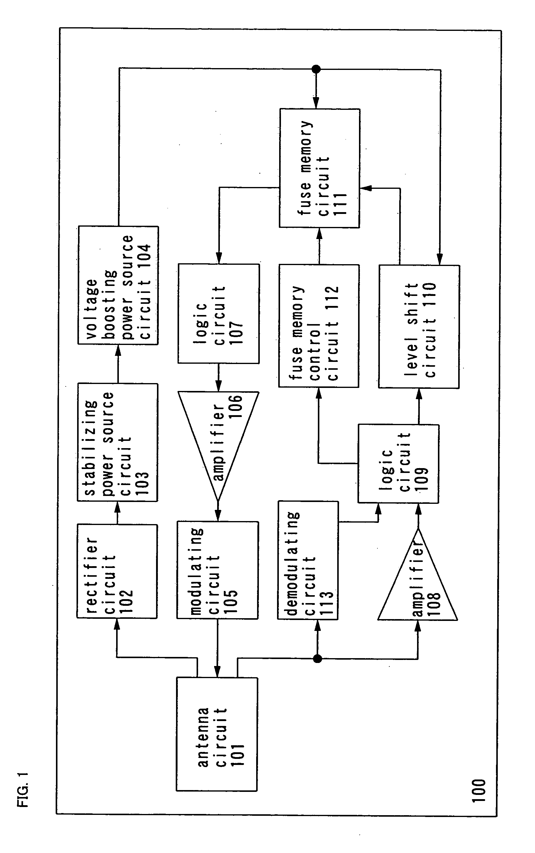
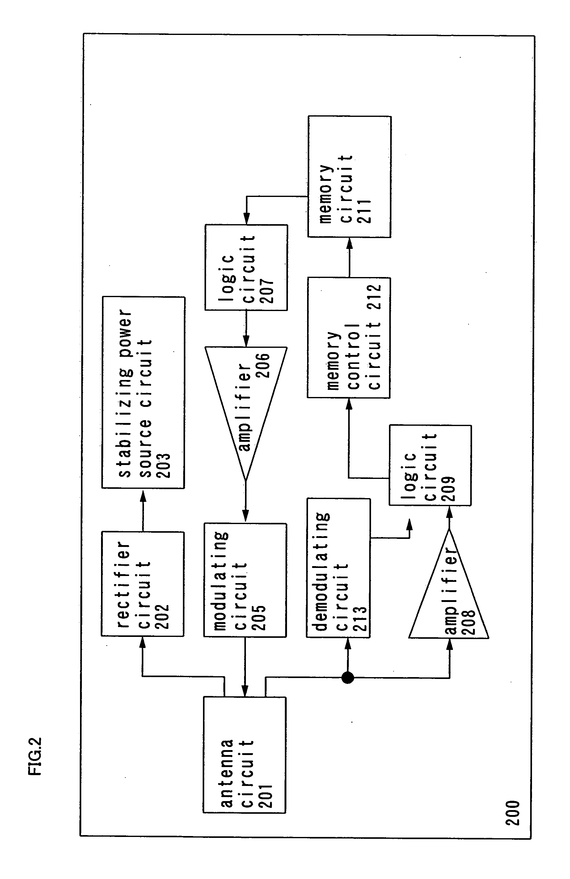
Semiconductor device
- Summary
- Abstract
- Description
- Claims
- Application Information
AI Technical Summary
Benefits of technology
Problems solved by technology
Method used
Image

Examples
embodiment 1
[0083] A fuse element is exemplary described using FIG. 6A. The fuse element shown in FIG. 6A is used by being blown its metal wiring like a general electronic fuse. As for the wiring material, a material for a gate electrode or a material for a source / drain electrode forming a thin film transistor (hereafter a TFT) can be employed. In order to blow with less heat generation, the width of the wiring is made as narrow as possible, and preferably 1 μm or less.
[0084] A fuse element using an island-shaped region of a TFT is described using FIG. 6B now. The fuse element shown in FIG. 6B flows a large amount of current. Therefore, a large amount of an N-type or P-type impurity is preferably added to suppress a resistance value thereof. In order to blow with less heat generation, the width of the wiring is made as narrow as possible, and preferably 1 μm or less.
embodiment 2
[0085] An embodiment of a fuse memory circuit using a fuse memory element which differs from the above-described one is described in FIG. 7. The fuse element in FIG. 7 uses a capacitor, which serves as a capacitor and is open with respect to direct current at the initial stage. When writing is over, both terminals are short-circuited because high voltage is applied to both electrodes of the fuse element, which are provided on both sides of an insulating film, and it breaks the insulating film to short-circuit.
[0086] An operation of the fuse memory circuit is described using FIG. 7 below. The fuse memory circuit shown in FIG. 7 is a 6-bit memory circuit for simplification, though the invention is not limited to a 6-bit. The fuse memory circuit includes a column decoder 701, a row decoder 702, a voltage boosting power source circuit 703, an amplifier 704, N-type transistors 705 to 710, fuse elements 711 to 716, bit lines 717 to 719, word lines 720 and 721, column switches 722 to 724,...
embodiment 3
[0097] Described exemplary using FIG. 9 is the case where data is written to a fuse memory by an external high voltage power source 903, instead of generating high voltage by rectifying, stabilizing, and voltage-boosting an input signal from an antenna. In FIG. 9, the fuse element used by being blown a resistor shown in FIG. 5 is employed, though the fuse element used by being short-circuited a capacitor shown in FIG. 7 may employed as well. Such a writing by means of the external high voltage power source 903 is suitable for the case where data is written while the chip is inspected. A test apparatus for an LSI is generally equipped with a high voltage power source, which can be used to write data. After an electrical inspection of the chip, a pad 930 is connected to the external high voltage power source 903 through an inspection probe, so that writing can be carried out. An operation thereof is described below.
[0098] The fuse memory circuit includes a column decoder 901, a row d...
PUM
 Abstract
Description
Claims
Application Information