Semiconductor device and manufacturing method thereof, liquid crystal television system, and EL television system

a technology of semiconductor devices and manufacturing methods, applied in television systems, non-linear optics, instruments, etc., can solve the problems of increasing the area of tft, reducing the throughput of the forming process, and wasting the most of the materials of film patterns and resists, etc., to achieve the control of thickness and width of the pattern to be formed, increase the w/l, and the effect of increasing the driving ability

Inactive Publication Date: 2005-08-18
SEMICON ENERGY LAB CO LTD
View PDF23 Cites 56 Cited by
  • Summary
  • Abstract
  • Description
  • Claims
  • Application Information

AI Technical Summary

Benefits of technology

[0033] As in the present invention, when a film pattern such as a wiring layer for a device, a conductive layer for forming an electrode, a semiconductor layer, or a mask layer for forming a predetermined pattern is formed by using droplet discharge, droplets can be discharged on any position by changing a nozzle that is a discharge nozzle for droplets including the material of the film and a substrate in relative position. In addition, depending on the nozzle size, the discharge amount of droplet, and the relative relation between the mobility speeds of the nozzle and a substrate on which discharged droplets are formed, the thickness and width of the pattern to be fo

Problems solved by technology

However, the process of forming a film pattern by using the conventional photolithography process has problems that most of the materials of the film pattern and resist are wasted and the number of processes for forming the mask pattern is large to decrease the throughput.
However, this structure has a problem that the area of the TFT is increased.
Therefore, the increase of the area of the TFT has a problem that the display region of the pixel region is limited to decrease t

Method used


Image

  • Semiconductor device and manufacturing method thereof, liquid crystal television system, and EL television system
  • Semiconductor device and manufacturing method thereof, liquid crystal television system, and EL television system
  • Semiconductor device and manufacturing method thereof, liquid crystal television system, and EL television system

Examples


embodiment mode 1

(Embodiment Mode 1)

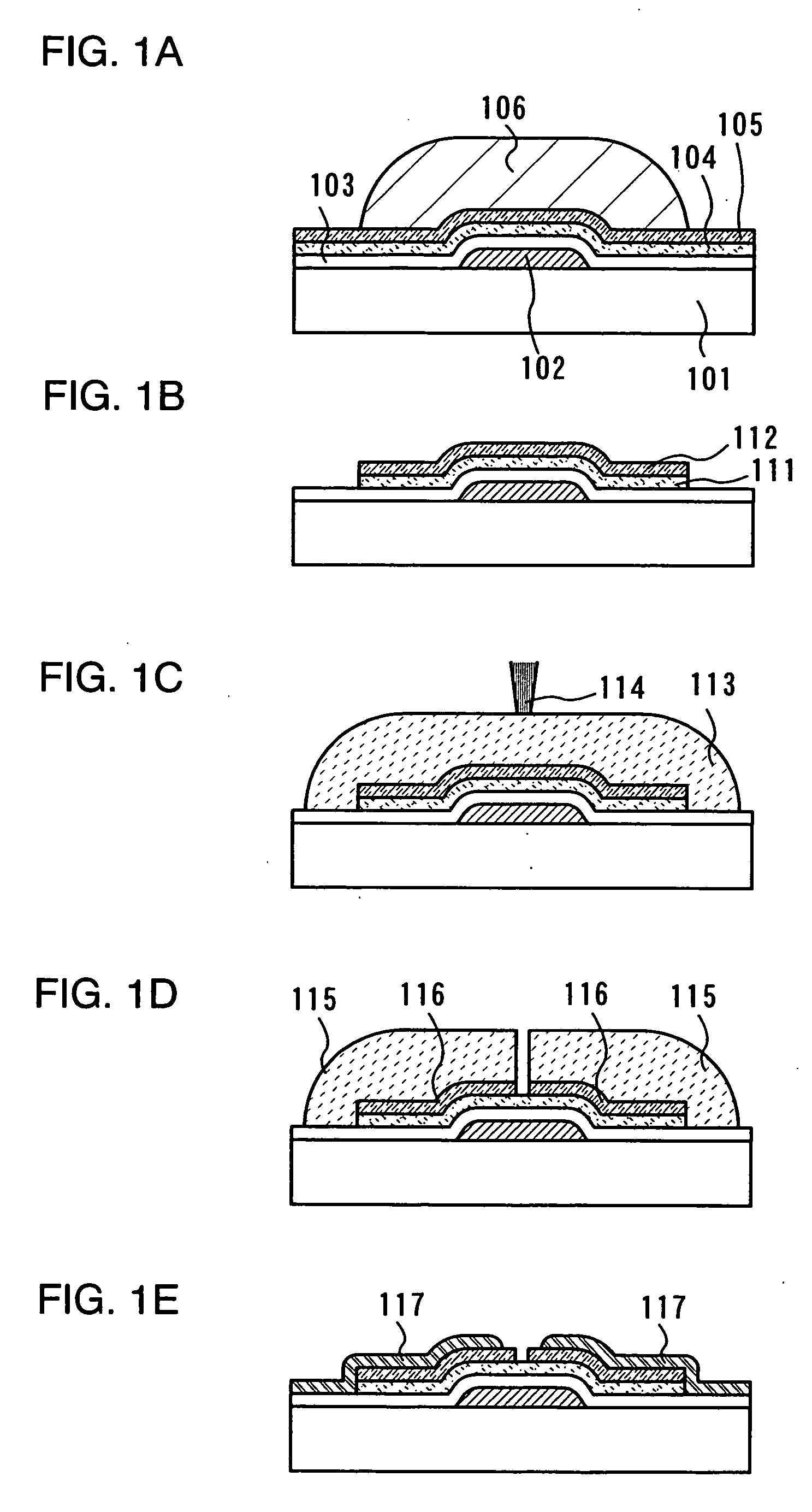
[0079] In this embodiment mode, a process will be described with reference to FIGS. 1A to 1E, where a mask pattern that is formed by irradiation with a laser beam (hereinafter, also referred to as laser light) is used to form a TFT with a short channel length.

[0080] Specifically, a process for forming a channel etch type TFT, which is one of inverted-staggered TFTs, as a semiconductor element will be described in this embodiment.

[0081] As shown in FIG. 1A, a first conductive layer 102 is formed over a substrate 101. As a method for forming the first conductive layer 102, droplet discharge, printing, electrolytic plating, PVD, or CVD is used. For example, in the case of employing PVD ore CVD, the first conductive layer 102 can be formed in such a way that a conductive layer is formed over the substrate 101, a photosensitive resin is formed thereon, the photosensitive resin is irradiated with laser light and developed to form a mask pattern, and then the conductiv...

embodiment mode 2

(Embodiment Mode 2)

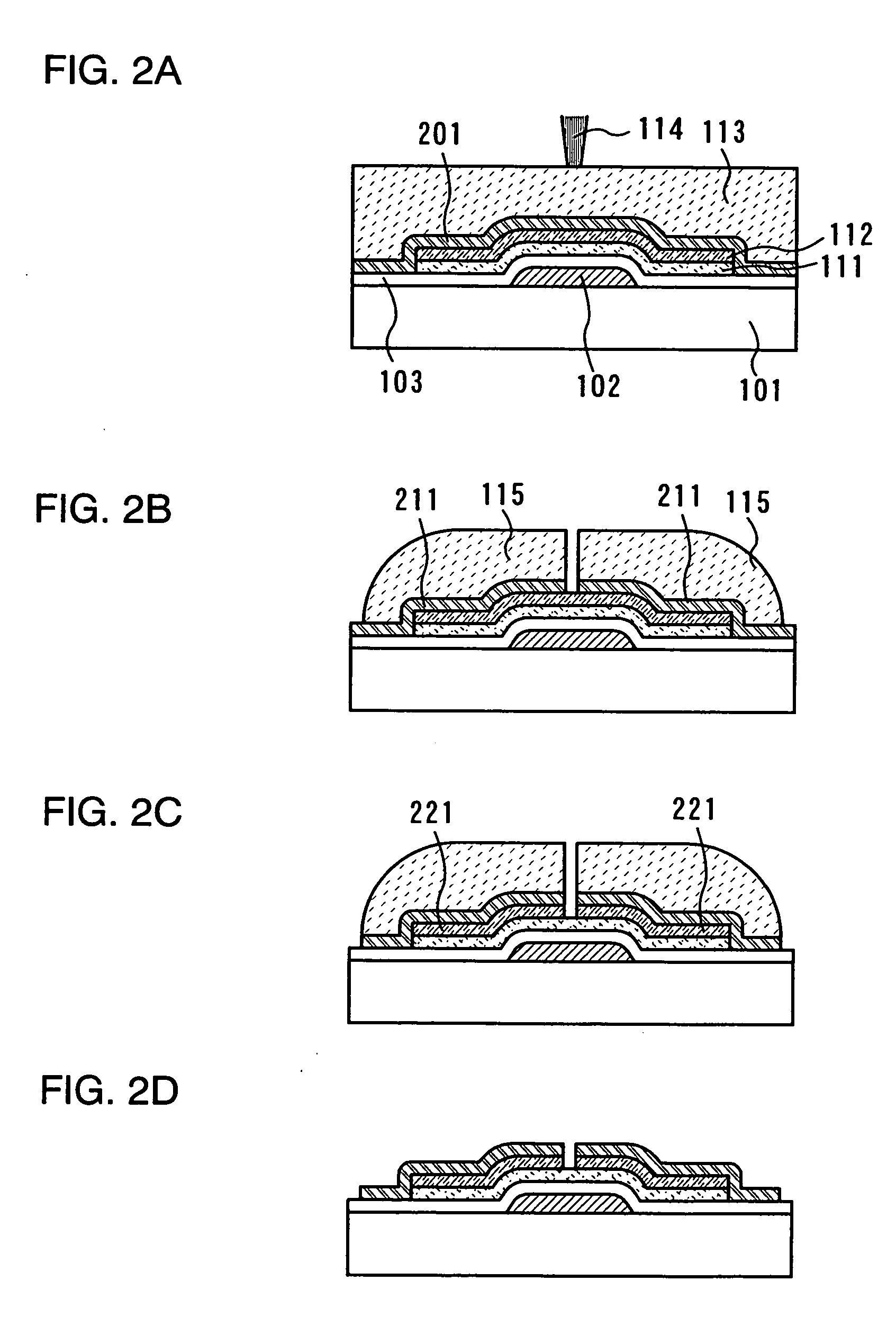
[0130] In this embodiment mode, with reference to FIGS. 2A to 2D, a process for forming a channel etch type TFT as in Embodiment Mode 1 will be described. This embodiment mode is different from Embodiment Mode 1 in the process for manufacturing the source electrode and the drain electrode.

[0131] As shown in FIG. 2A, a first conductive layer 102, a first insulating layer 103, a first semiconductor region 111, and a second semiconductor region 112 are formed over a substrate 101 in the same way as in Embodiment Mode 1.

[0132] Next, a second conductive film 201 is formed on the second semiconductor region 112 and the first insulating film 103. The material and manufacturing process of the second conductive film 201 can be the same as those of the first conductive layer 102 in the Embodiment Mode 1.

[0133] Next, a photosensitive resin 113 is applied or discharged over the substrate, and then the photosensitive resin 113 is irradiated with laser light 114 for exposure...

embodiment mode 3

(Embodiment Mode 3)

[0137] In this embodiment mode, with reference to FIGS. 3A to 3E, a process for forming a channel etch type TFT with a short channel length by using a material forming a liquid-repellent surface will be described. In this embodiment mode, source and drain regions are formed by forming a mask pattern on a second semiconductor film that is conductive and etching the second semiconductor film with the use of this mask pattern.

[0138] As shown in FIG. 2A, a first conductive layer 102, a first insulating layer 103, and a first semiconductor film are formed over a substrate 101 in the same way as in Embodiment Mode 1. After that, a first semiconductor region 111 is formed by forming a first mask pattern 106 as shown in Embodiment Mode 1 and etching the first semiconductor film.

[0139] Next, a second semiconductor film 301 is formed on the first semiconductor region 111 and the first insulating film 103. The material and manufacturing method of the second semiconductor f...


PUM


Abstract

It is an object of the present invention to provide a method for manufacturing a semiconductor device that has high driving ability (that is, large W/L) according to a method in which the use efficiency of a material is improved and the throughput and yield are enhanced. The present invention provides a method for a semiconductor device, which comprises the steps of forming a first conductive layer in contact with a semiconductor region, forming an insulating layer on the first conductive layer by one of droplet discharge and application, irradiating a portion of the insulating layer with laser light to form a mask pattern, and forming divided first conductive layers by etching with the use of the mask pattern as a mask.

Description

BACKGROUND OF THE INVENTION [0001] 1. Field of the Invention [0002] The present invention relates to a method for manufacturing a semiconductor device by using droplet discharge typified by ink-jet. [0003] 2. Description of the Related Art [0004] In manufacture of semiconductor devices, the use of droplet discharge has been examined for development of producing technologies by which a plurality of display panels is taken from one mother glass substrate for efficient mass production. [0005] In order to form a film pattern for a conventional semiconductor device, a method for forming a film pattern is used, where a film (a film comprising a semiconductor material, an insulator material, or a conductive material) at a portion to be the film pattern is removed by etching with a resist pattern as a mask pattern after a photolithography process of forming the resist pattern by applying a resist on the whole area of a substrate, pre-baking the applied resist, and then, irradiation with lig...

Claims


Application Information

Patent Timeline
IPC IPC(8): B41J2/015G02F1/136G03F7/20H01L21/027H01L21/336H01L21/77H01L21/84H01L27/12H01L29/10H01L29/417H01L29/423H01L29/76H01L29/786H04N5/44
CPCH01L27/1292H01L29/41733H01L2924/07811H01L2224/48091H01L2924/10253H01L29/78648H01L2924/01087H01L2924/01068H01L2924/01067H01L2924/01055H01L2924/01019H01L2224/73265H01L2224/73204H01L2224/48465H01L2224/48227H01L2224/32225H01L2224/16225H01L2924/3025H01L2924/19041H01L2924/04941H01L2924/01079H01L2924/01078H01L2924/01077H01L2924/01046H01L29/42384H01L29/66765H01L29/78645H01L29/78678H01L29/78696H01L2924/01004H01L2924/01012H01L2924/0102H01L2924/01025H01L2924/01029H01L2924/00012H01L2924/00H01L2924/00014H01L24/05H01L24/73H01L2224/05001H01L2224/05008H01L2224/05024H01L2224/05572H01L2224/05666H01L2224/05681H01L2924/12044H01L2924/14H01L2924/181
Inventor YAMAZAKI, SHUNPEISUZUKI, YUKIE
Owner SEMICON ENERGY LAB CO LTD
Why Eureka
Try Eureka