Memory device using nano tube cell
a memory device and nanotube technology, applied in nanoinformatics, instruments, animal intestines working up, etc., can solve the problems of junction leakage current generation and difficulty in satisfying the refresh characteristic of dram cells, and achieve the effect of reducing the capacitance of each cell and reducing the size of a capacitor
- Summary
- Abstract
- Description
- Claims
- Application Information
AI Technical Summary
Benefits of technology
Problems solved by technology
Method used
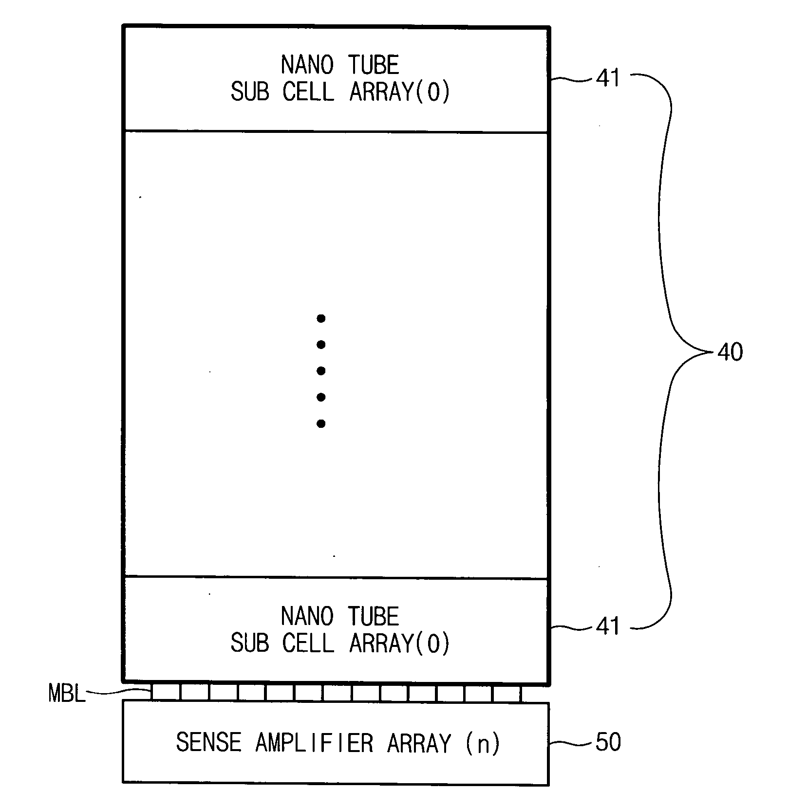
Image

Examples
Embodiment Construction
[0024] The present invention will be described in detail with reference to the accompanying drawings.
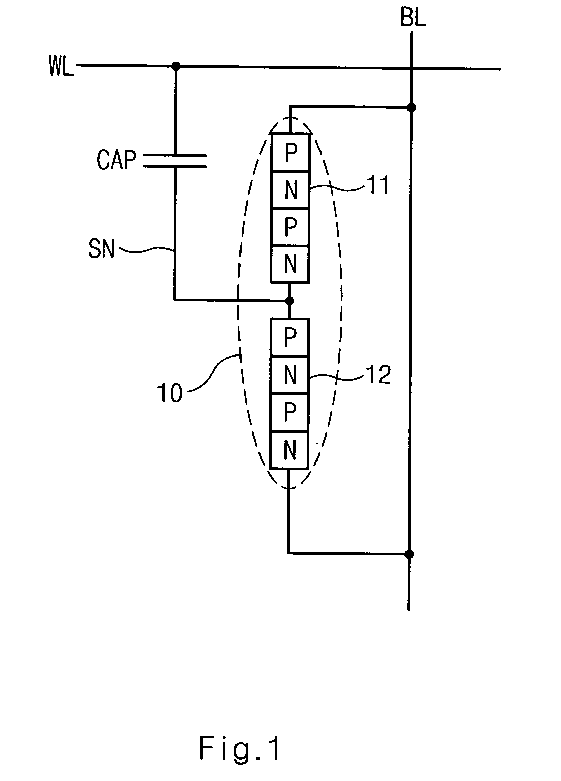
[0025]FIG. 1 is a diagram illustrating a unit nano tube cell according to an embodiment of the present invention.
[0026] In an embodiment, the unit nano tube cell comprises a capacitor CAP and a PNPN nano tube switch 10. Here, the PNPN nano tube switch 10 comprises PNPN diode switches 11 and 12. The PNPN diode switches 11 and 12 are connected in parallel between a bit line BL and a bottom electrode of the capacitor CAP.
[0027] The PNPN diode switch 11 is connected backward between the bit line BL and one electrode of the capacitor CAP, and the PNPN diode switch 12 is connected forward between the bit line BL and one electrode of the capacitor CAP. The other electrode of the capacitor CAP is connected to a word line WL.
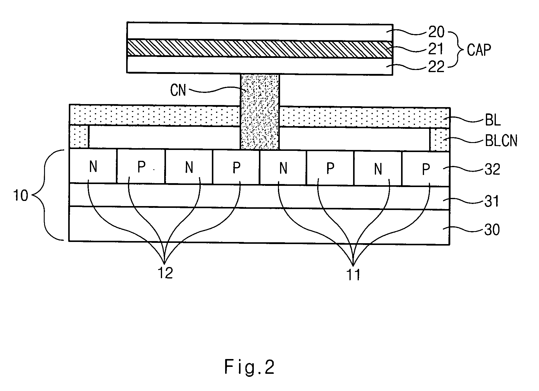
[0028]FIG. 2 is a cross-sectional diagram illustrating the nano tube cell of FIG. 1.
[0029] The PNPN nano tube switch 10 comprises an insulating layer 31 formed on a ...
PUM
 Abstract
Description
Claims
Application Information
 - R&D
- Intellectual Property
- Life Sciences
- Materials
- Tech Scout
- Unparalleled Data Quality
- Higher Quality Content
- 60% Fewer Hallucinations
Browse by: Latest US Patents, China's latest patents, Technical Efficacy Thesaurus, Application Domain, Technology Topic, Popular Technical Reports.
© 2025 PatSnap. All rights reserved.Legal|Privacy policy|Modern Slavery Act Transparency Statement|Sitemap|About US| Contact US: help@patsnap.com