Strained-channel semiconductor structure and method of fabricating the same

a strain-channel semiconductor and fabrication method technology, applied in the field of strain-channel semiconductor structure and the field of fabricating the same, can solve the problems of high defect density, high cost of approach, and possible strain relaxation

Inactive Publication Date: 2005-08-25
TAIWAN SEMICON MFG CO LTD
View PDF4 Cites 138 Cited by
  • Summary
  • Abstract
  • Description
  • Claims
  • Application Information

AI Technical Summary

Benefits of technology

[0020] Another object of the present invention is to provide a strained-channel semiconductor structure having at least one strained-channel transistor. The outer side of the lattice-mismatched zones of the source / drain regions thereof on each end laterally contacts the first semiconductor material of the adjacent substrate such that strain exerted thereof will not be buffered or reduced by the material of the adjacent isolation region.

Problems solved by technology

Hence, there are concerns about possible strain relaxation resulting from subsequent high temperature CMOS processes.
Further, the approach is very expensive as the SiGe buffer layer 110 with a thickness on the order of micrometers must be grown.
Numerous dislocations exist in relaxed SiGe layer 114, some of which propagate to the strained-Si layer 130, resulting in high defect density, thereby negatively affecting transistor performance.

Method used


Image

  • Strained-channel semiconductor structure and method of fabricating the same
  • Strained-channel semiconductor structure and method of fabricating the same
  • Strained-channel semiconductor structure and method of fabricating the same

Examples


first embodiment

[0054] A method of fabricating the strained-channel semiconductor structure of the invention is illustrated in FIGS. 4a to 4h.

[0055] In FIG. 4a, a substrate 300 of a first semiconductor material is provided. The substrate 300 may comprise a plurality of active areas (not shown) for forming devices thereon defined by a plurality of isolation structures (not shown) formed in the substrate 300, however an active area AA defined by two adjacent isolation regions 302 shown in FIG. 4a is provided to simplify the description. The first semiconductor material of the substrate 300 can be elemental, alloy or compound semiconductor material and is preferably an elemental semiconductor material such as silicon. The isolation region 302 can be, for example, a conventional shallow trench isolation (STI) region.

[0056] Next, a first gate stack G including a gate dielectric layer 304, a gate electrode layer 306, and a mask layer 308 sequentially stacked over a portion of the substrate 300 is forme...

second embodiment

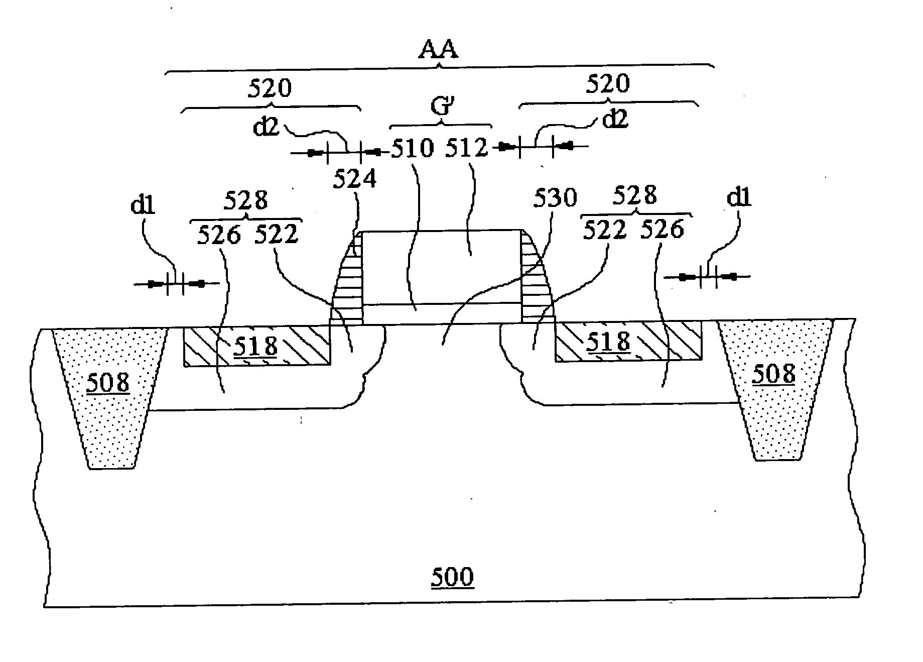
[0075] The method of fabricating the strained-channel semiconductor structure illustrated in FIGS. 4a through 4h of the first embodiment of the present invention can also be applied to the application of forming a transistor array having a plurality of strained-channel transistors on a substrate.

[0076] Structures of the strained-channel semiconductor structure having a transistor array thereon are shown in FIGS. 5a and 5b to respectively illustrate a strained-channel transistor array formed over an active area AA defined by one or two isolation regions 302 in the substrate 300. Each transistor formed in the active area AA is illustrated as the strained-channel transistor 30a shown in FIG. 4c, for example. The gate structures (referring to the second gate structures G′) and adjacent source / drain regions 324 comprising the lattice-mismatched zone 314 are alternatively disposed on and in the substrate 300, forming a transistor array connected to functional circuits such as NOR circuit...

third embodiment

[0079] Another method of fabricating the strained-channel semiconductor structure of the invention is illustrated in FIGS. 6a to 6h.

[0080] In FIG. 6a, a substrate 400 of first semiconductor material is provided. The substrate 400 may comprise a plurality of active areas (not shown) for forming devices thereon defined by a plurality of isolation structures (not shown) formed in the substrate 400. The active area AA defined by two adjacent isolation regions 402 is shown in FIG. 6a to simplify the description. The first semiconductor material of the substrate 400 can be elemental, alloy or compound semiconductor material and is preferably an elemental semiconductor material such as silicon. The isolation region 402 can be, for example, a conventional shallow trench isolation (STI) region.

[0081] Next, a first gate stack G including a gate dielectric layer 404, a gate electrode layer 406, and a mask layer 408 sequentially stacked over a portion of the substrate 400 is formed in the act...


PUM


Abstract

A strained-channel semiconductor structure and method of fabricating the same. The strained-channel semiconductor structure comprises a substrate composed of a first semiconductor material with a first natural lattice constant. A channel region is disposed in the substrate and a gate stack is disposed over the strained channel region A pair of source / drain regions are oppositely disposed in the substrate adjacent to the channel region, wherein each of the source / drain regions comprises a lattice-mismatched zone comprising a second semiconductor material with a second natural lattice constant rather than the first natural lattice constant, an inner side and an outer side corresponding to the gate stack, and at least one outer sides laterally contacts the first semiconductor material of the substrate.

Description

BACKGROUND OF THE INVENTION [0001] 1. Field of the Invention [0002] The present invention relates to a semiconductor structure. More particularly, it relates to a strained-channel semiconductor structure and method of fabricating the same. [0003] 2. Description of the Related Art [0004] Size reduction of the metal-oxide-semiconductor field-effect transistor (MOSFET), including reduction of gate length and gate oxide thickness, has enabled continuous improvement in performance, reduced density, and cost per unit of integrated circuits. [0005] In order to further enhance transistor performance, strain can be introduced in the transistor channel to improve carrier mobility and device scaling. There are several existing approaches to introducing strain in a transistor channel region. [0006] In one conventional approach, as described in the paper entitled “NMOS and PMOS transistors fabricated in strained silicon / relaxed silicon-germanium structures”, by J. Welser et al., published at the...

Claims


Application Information

Patent Timeline
Patent Type & Authority Applications(United States)
IPC IPC(8): H01L21/336H01L21/8234H01L29/08H01L29/51H01L29/76H01L29/78
CPCH01L21/823412H01L21/823418H01L21/823425H01L29/0847H01L29/41783H01L29/517Y10S438/938H01L29/6659H01L29/66636H01L29/7833H01L29/7842H01L29/7848H01L29/665
Inventor LIN, CHUN-CHIEHYEO, YEE-CHIA
Owner TAIWAN SEMICON MFG CO LTD
Why Eureka
Try Eureka