Method of manufacturing semiconductor device

a manufacturing method and semiconductor technology, applied in the direction of transistors, electrical devices, basic electric elements, etc., can solve the problems of low concentration of impurities in the ldd region and more serious problems

Inactive Publication Date: 2005-08-25
KK TOSHIBA
View PDF16 Cites 9 Cited by
  • Summary
  • Abstract
  • Description
  • Claims
  • Application Information

AI Technical Summary

Benefits of technology

[0014] A method of manufacturing a semiconductor device including a plurality of MIS (metal insulator semiconductor) transistors formed on a semiconductor substrate, according to the first aspect of the present invention, comprises: forming a plurality of gate electrodes associated with the MIS transistors on the semiconductor substrate, with a plurality of gate insulating films interposed between the gate electrodes and the semiconductor substrate, respectively; and successively forming a plurality of impurity diffusion regions for lightly doped drain (LDD) regions in the semiconductor substrate, at decreasing junction depths, respectively, by using lithography and ion implantation, such that each of the impurity diffusion regions being provided on both sides of a respective one of the gate electrodes.

Problems solved by technology

This problem is more serious when the concentration of the impurities doped in the LDD regions is low.

Method used


Image

  • Method of manufacturing semiconductor device
  • Method of manufacturing semiconductor device
  • Method of manufacturing semiconductor device

Examples


first embodiment

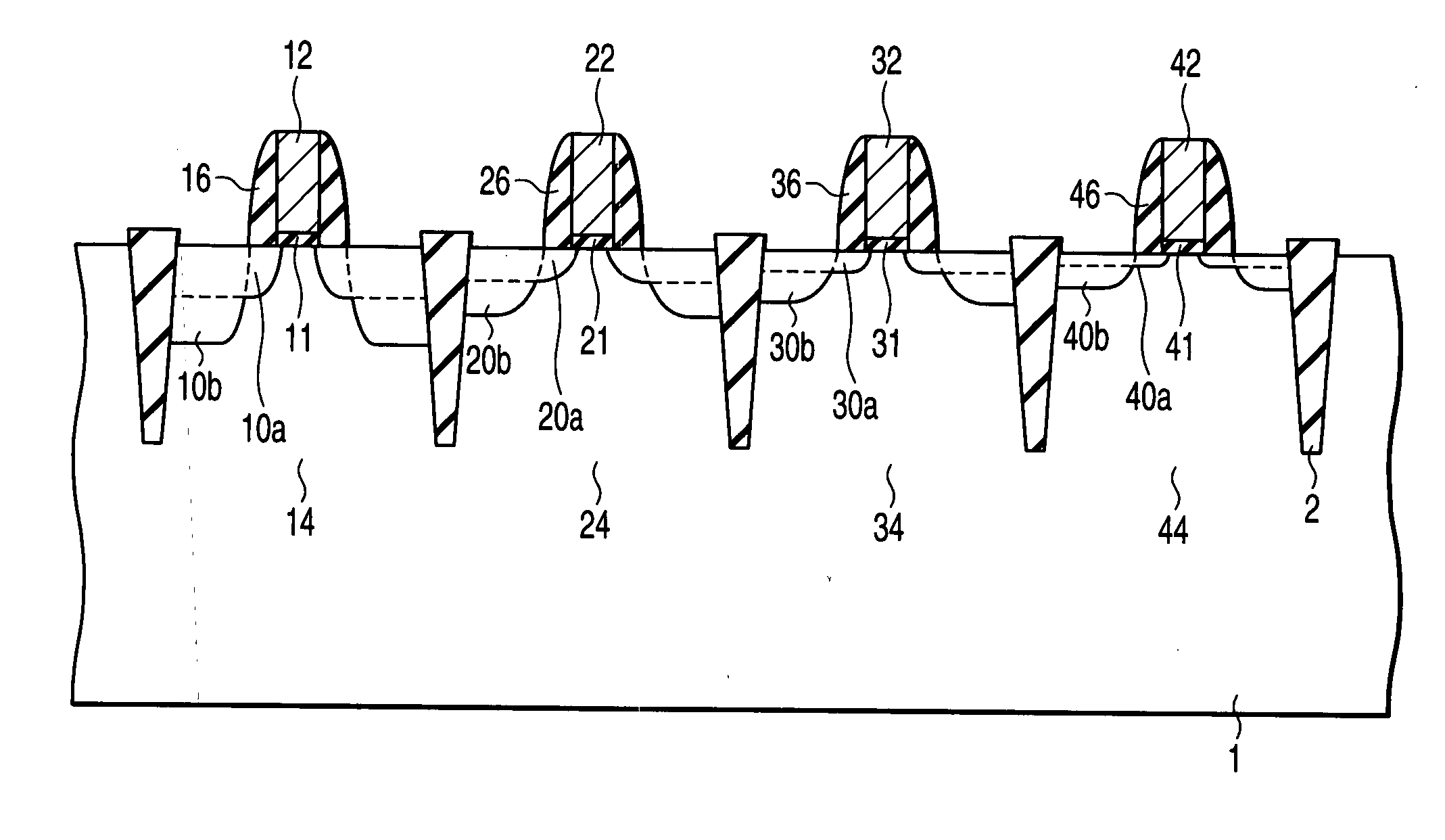
[0038]FIG. 1 is a cross-sectional view of a semiconductor device according to the first embodiment of the present invention. To be more specific, FIG. 1 is a cross-sectional view of low-concentration impurity diffusion regions (which will be hereinafter referred to as low-concentration impurity regions) before formations of deep source and drain regions. Part of the low-concentration impurity regions will become LDD region layers.

[0039] The LDD regions are impurity diffusion layers having a relatively low concentration, which are formed at end portions of a drain region and a source region of a MOS transistor, which are located adjacent to the channel. When a MOS transistor is formed to include such LDD regions, an electric field concentratedly generated at the end portion of the drain region is reduced, thus restricting a hot carrier effect.

[0040] More specifically, when the LDD regions are provided in the above manner, resistor element is connected between the channel and drain ...

second embodiment

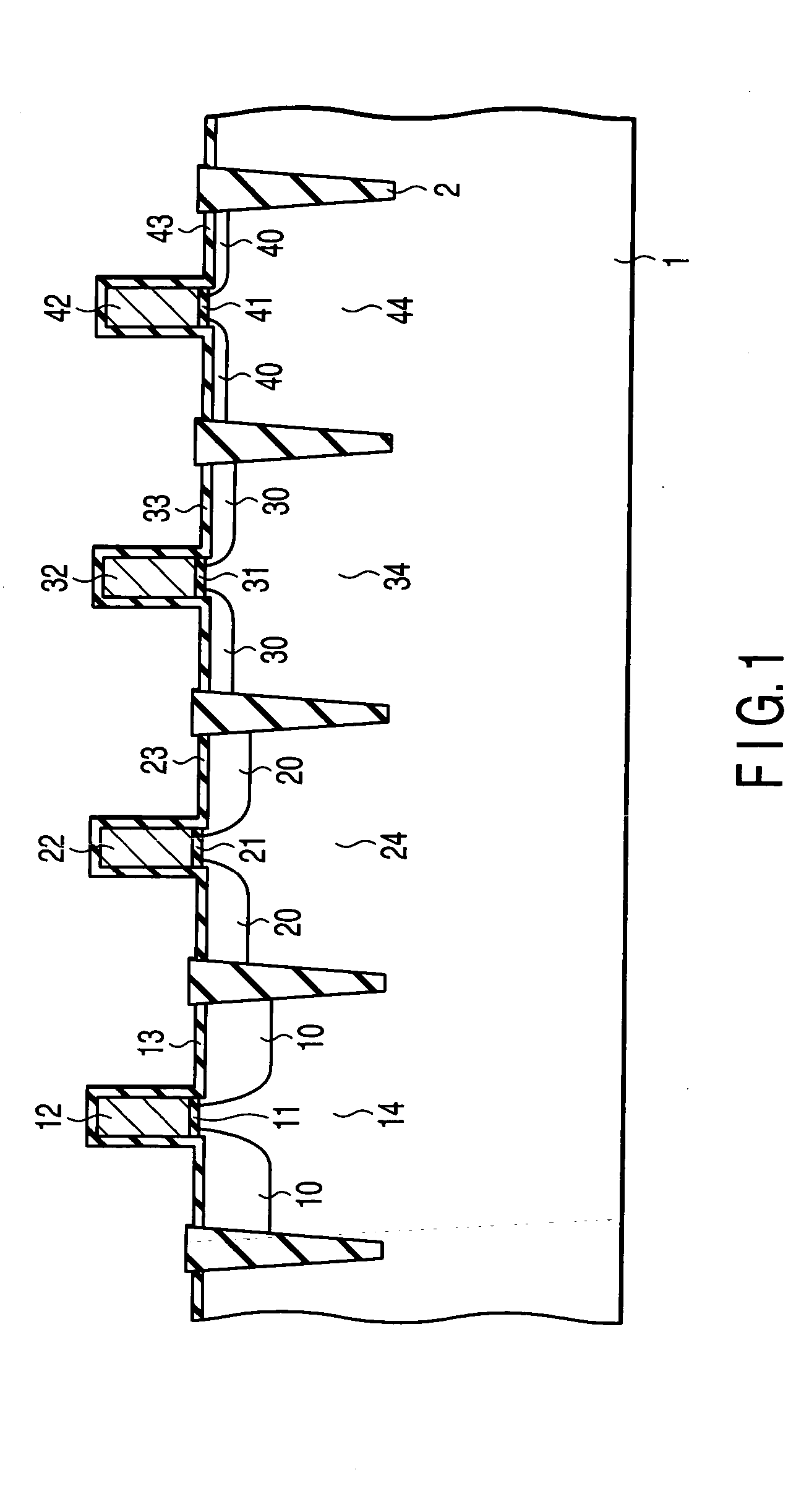
[0086]FIG. 13 is a cross-sectional view of a semiconductor device according to the second embodiment of the present invention.

[0087] In the second embodiment, low-concentration impurity regions 10, 20, 50 and 60 having different junction depths are formed on the same semiconductor substrate 1. The junction depth of the low-concentration impurity regions 10 is larger than that of the low-concentration impurity regions 20, which is larger than that of the low-concentration impurity regions 50. The junction depth of the low-concentration impurity regions 50 is substantially equal to that of the low-concentration impurity regions 60.

[0088] The low-concentration impurity regions 50 are different from the low-concentration impurity regions 60 regarding the depth at which the impurity concentration is peak in the impurity density distribution of the low-concentration impurity regions. FIG. 14 is a cross-sectional view showing depths at which the impurity concentrations of the low-concent...


PUM


Abstract

A method of manufacturing a semiconductor device including a plurality of MIS transistors formed on a semiconductor substrate, includes forming a plurality of gate electrodes associated with the MIS transistors on the semiconductor substrate, with a plurality of gate insulating films interposed between the gate electrodes and the semiconductor substrate, respectively, and successively forming a plurality of impurity diffusion regions for LDD regions in the semiconductor substrate, at decreasing junction depths, respectively, by using lithography and ion implantation, such that each of the impurity diffusion regions being provided on both sides of a respective one of the gate electrodes.

Description

CROSS-REFERENCE TO RELATED APPLICATIONS [0001] This application is based upon and claims the benefit of priority from prior Japanese Patent Application No. 2004-013992, filed Jan. 22, 2004, the entire contents of which are incorporated herein by reference. BACKGROUND OF THE INVENTION [0002] 1. Field of the Invention [0003] The present invention relates to a method of manufacturing a semiconductor device, and in particular a semiconductor device provided with a metal oxide semiconductor (MOS) having a lightly doped drain (LDD) structure. [0004] 2. Description of the Related Art [0005] In recent years, semiconductor integrated circuits have been formed at a higher density, and have also been made smaller. Under such circumstances, semiconductor integrated circuits employ an LDD structure as the structures of MOS transistors to restrict the short channel effect of the MOS transistors, and improve the driving function of the MOS transistors. [0006] In the LDD structure, regions whose im...

Claims


Application Information

Patent Timeline
Patent Type & Authority Applications(United States)
IPC IPC(8): H01L21/336H01L21/8234H01L27/088
CPCH01L21/823418H01L29/6659H01L21/823481
Inventor HASUMI, RYOJIMIYASHITA, KATSURA
Owner KK TOSHIBA
Why Eureka
Try Eureka