RFID-UHF integrated circuit

a technology of integrated circuits and integrated circuits, which is applied in the direction of transmission systems, transmission, indirect connection of subscribers, etc., can solve the problems of inability to carry (or attach to) living beings (human beings, animals), cannot be used in water or metal, and is difficult to envisage writing data in passive-type uhf circuits, and cannot be powered by any electrical power source. , to achieve the effect of avoiding the possibility of incorporating a voltage sour

Active Publication Date: 2005-08-25
WISEKEY SEMICONDUCTORS
View PDF6 Cites 103 Cited by
  • Summary
  • Abstract
  • Description
  • Claims
  • Application Information

AI Technical Summary

Problems solved by technology

One essential difference between RFID integrated circuits and UHF integrated circuits is that the latter cannot be carried by (or attached to) living beings (human beings, animals) and do not work in the presence of water or metal.
Furthermore, it is difficult to envisage writing data in passive-type UHF circuits (without any source of electrical power) since the electrical power that can be extracted from the UHF electric field is too low to generate a high voltage Vpp for erasing and programming an EEPROM or a FLASH memory.
Now, in most applications, it is not possible to consider incorporating a voltage source into a UHF electronic tag that enables the memory to be written without restricting the communication distance, both for reasons of encumbrance and cost price and for reasons of product service life, such that most UHF integrated circuits are of the passive type.
Furthermore, it is not possible to extract a clock signal from the UHF signal for technological reasons (frequency too high to be applied to a frequency divider) and the synchronisation of the data transfer requires the use of special coding of the data (synchronisation signal included in the coding of the bit).
But as their memory cannot be written in normal conditions of use, it is not possible to write traceability data (such as indications of product storage place and date, indications about transit, etc. for example).

Method used


Image

  • RFID-UHF integrated circuit
  • RFID-UHF integrated circuit
  • RFID-UHF integrated circuit

Examples


Embodiment Construction

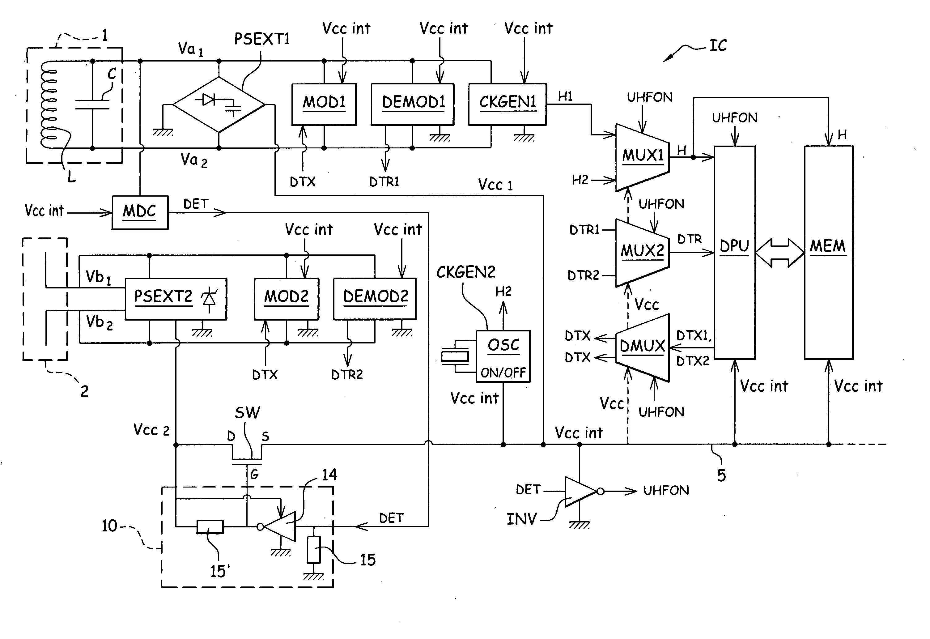
[0037]FIG. 1 represents the architecture of an integrated circuit IC according to the present invention. The integrated circuit comprises a first analog interface comprising an RF antenna circuit referenced 1, an electrical supply circuit PSEXT1, a clock generator CKGEN1, a modulation circuit MOD1 and a demodulation circuit DEMOD1.

[0038] The antenna circuit 1 comprises at least one coil L and one tuning capacitor C, the assembly here being tuned to a resonance frequency in the order of 13.56 MHz. The coil L may comprise one or more windings, and may also comprise a first coil for receiving the electric energy and a second coil for transmitting the data.

[0039] The electrical supply circuit PSEXT1 is a diode rectifier that delivers a supply voltage Vcc1 using an induced alternating voltage Va of frequency 13.56 MHz. This voltage Va, which comprises a positive half-wave Va1 and a negative half-wave Va2, appears at the terminals of the antenna circuit 1 when the integrated circuit is ...


PUM


Abstract

The present invention relates to a contactless integrated circuit comprising an RFID communication interface comprising an antenna coil for receiving a first induced alternating voltage when the integrated circuit is in the presence of an RF magnetic field, and a data processing unit linked to the first communication interface, the data processing unit being equipped with an electrically programmable and erasable memory. According to the present invention the integrated circuit further comprises a UHF communication interface comprising a UHF antenna for receiving a second induced alternating voltage when the integrated circuit is in the presence of a UHF electric field signal, and a multiplexing means for linking the data processing unit to one or other of the two communication interfaces.

Description

CROSS-REFERENCE TO RELATED APPLICATIONS [0001] This application is a continuation of International Application No. PCT / FR2003 / 002938, filed Oct. 7, 2003, which was published in the French language on Apr. 22, 2004, under International Publication No. WO 2004 / 034317 A2, and the disclosure of which is incorporated herein by reference.BACKGROUND OF THE INVENTION [0002] The present invention relates to contactless integrated circuits operating by inductive coupling and contactless integrated circuits operating by electric field coupling. [0003] In recent years, contactless integrated circuits operating by inductive coupling, or RFID integrated circuits, have considerably developed. Table 1 below summarises the characteristics generally found and / or standardised for this type of contactless integrated circuit. TABLE 1main characteristics of RFID integrated circuitsOperating frequency: 13.56 MHz*Magnetic field radiation: WideData rate: 26, 106, 424, 847 Kbits / sClock signal extraction fro...

Claims


Application Information

Patent Timeline
Patent Type & Authority Applications(United States)
IPC IPC(8): G06K19/07H04B5/00H04B7/00H04Q5/22
CPCG06K19/07786G06K19/0723
Inventor KOWALSKI, JACEKSERRA, DIDIERCHARRAT, BRUNO
Owner WISEKEY SEMICONDUCTORS
Why Eureka
Try Eureka