Apparatus and methods for cooling semiconductor integrated circuit package structures

a technology of integrated circuit and package structure, which is applied in the direction of electrical apparatus, semiconductor devices, semiconductor/solid-state device details, etc., can solve the problems of increasing power density, limiting system performance, and unable to efficiently remove heat, so as to reduce thermal resistance, increase thermal conductivity, and high thermal conductivity

Inactive Publication Date: 2005-09-01
IBM CORP
View PDF28 Cites 11 Cited by
  • Summary
  • Abstract
  • Description
  • Claims
  • Application Information

AI Technical Summary

Benefits of technology

[0016] Exemplary embodiments of the invention generally include apparatus and methods for cooling semiconductor integrated circuit (IC) chip packages. More specifically, exemplary embodiments of the invention include apparatus and methods for thermally coupling a semiconductor chip directly to a heat conducting device, which is formed of a material having a high thermal conductivity (e.g., copper heat sink or package lid). Thermal coupling is achieved using a thermal joint that provides increased thermal conductivity (or reduced thermal resistance) of the thermal connection between the semiconductor chip and the heat conducting dev...

Problems solved by technology

The ability to efficiently remove heat becomes even more problematic as chip geometries are scaled down and operating speeds are increased, resulting in increased power density.
As such, the ability to effectively cool semiconductor chips is a factor that limits increases in system performance.
Less viscous thermally conductive materials, such as oils, have a lower thermal conductivity than pastes, but can also be applied in much thinner layers, resulting in improved thermal performance, but less mechanical compliance.
The ability to effectively use a rigid bond is limited not only by the difference in the TCEs of the materials that form the heat spreader and IC chip, but also on the temperature range (cycle) in which the semiconductor package will operate or be exposed to, as well as size of the area over which the rigid bond will be formed.
Moreover, effective heat removal is difficult for densely packed, high-powered devices.
For example, a multi-chip module (MCM) package which comprises an array of IC chips mounted face down on a common substrate, presents special cooling difficulties.
With such an arrangement, it may not be possible to use a heat spreader bonded directly to the back surface of the chips, as is sometimes used for isolated chips, to reduce the heat flux (power/unit area, i.e. W/cm2).
Furthermore, difficulties arise for efficient heat removal with respect to IC chips, such as processors, that have “hot spot” regions, which can have a heat flux significantly greater than the average heat flux, resulting in temperatures ˜20° C. hotter than the average chip temperature.
A thermal solution that may be adequate for efficient...

Method used


Image

  • Apparatus and methods for cooling semiconductor integrated circuit package structures
  • Apparatus and methods for cooling semiconductor integrated circuit package structures
  • Apparatus and methods for cooling semiconductor integrated circuit package structures

Examples


Embodiment Construction

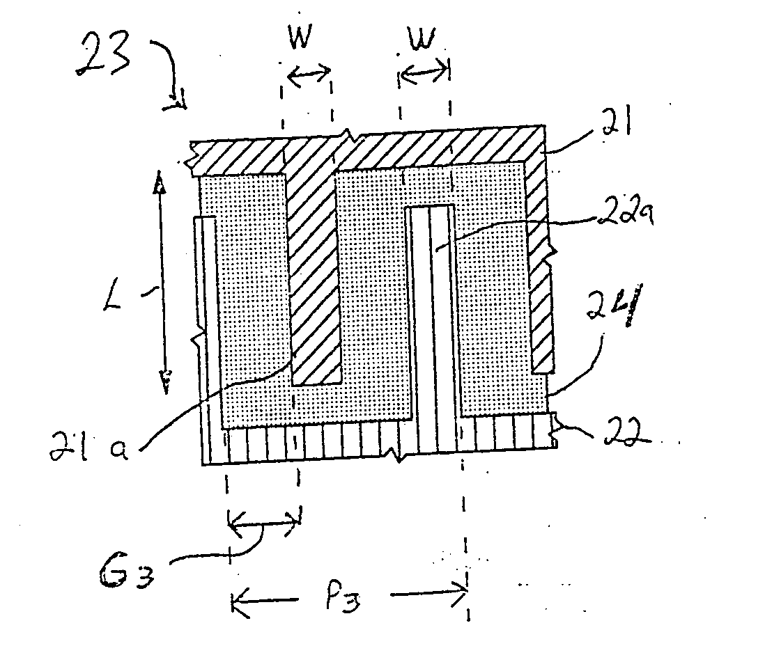
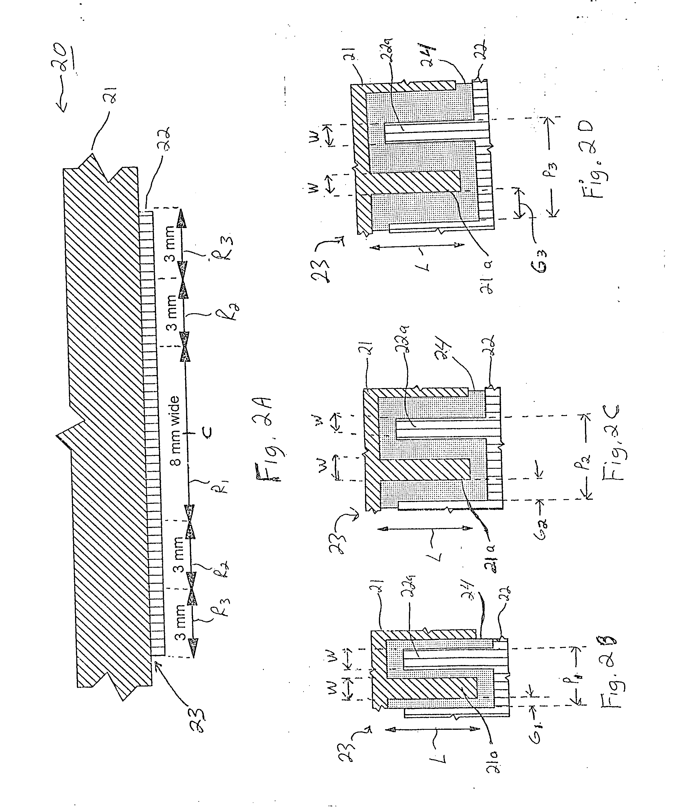
[0036] In general, exemplary embodiments of the invention include apparatus and methods for cooling semiconductor integrated circuit (IC) chip packages. More specifically, exemplary embodiments of the invention include apparatus and methods for thermally coupling a semiconductor chip directly to a heat conducting device, which is formed of a material having a high thermal conductivity (e.g., copper heat sink or package lid). Thermal coupling is achieved using a thermal joint that provides increased thermal conductivity (or reduced thermal resistance) of the thermal connection between the semiconductor chip and the heat conducting device, while minimizing or eliminating mechanical stress at the thermal joint caused by the relative displacement between the semiconductor chip and heat conducting device with temperature cycling due to differences in thermal expansion between the chip and heat conducting device over a wide temperature range. Moreover, exemplary embodiments of the inventi...


PUM


Abstract

Apparatus and methods are provided for thermally coupling a semiconductor chip directly to a heat conducting device (e.g., a copper heat sink) using a thermal joint that provides increased thermal conductivity between the heat conducting device and high power density regions of the semiconductor chip, while minimizing or eliminating mechanical stress due to the relative displacement due to the difference in thermal expansion between the semiconductor chip and the heat conducting device.

Description

TECHNICAL FILED OF THE INVENTION [0001] The present invention relates generally to apparatus and methods for cooling semiconductor integrated circuit (IC) chip packages. More specifically, the present invention relates to apparatus and methods for thermally coupling a semiconductor chip directly to a heat conducting device (e.g., a copper heat sink) using a thermal joint that provides increased thermal conductivity between the heat conducting device and high power density regions of the semiconductor chip, while minimizing or eliminating mechanical stress from the relative displacement with temperature cycling due to the differences in thermal expansion between the semiconductor chip and the heat conducting device. BACKGROUND [0002] In the design and manufacture of semiconductor IC (integrated circuit) chip packages and modules, it is imperative to consider and implement mechanisms that can effectively remove heat that is generated during operation of the IC chip devices (e.g., tran...

Claims


Application Information

Patent Timeline
IPC IPC(8): H01L23/367H01L29/739
CPCH01L23/367H01L2924/0002H01L2924/00
Inventor COLGAN, EVAN GEORGEGELORME, JEFFREY D.SIKKA, KAMAL K.TOY, HILTON T.ZITZ, JEFFREY ALLEN
Owner IBM CORP
Why Eureka
Try Eureka