Germanium deposition

a germanium film and film technology, applied in the direction of crystal growth process, polycrystalline material growth, chemically reactive gas, etc., can solve the problems of reducing device performance and device failure, reducing carrier mobility, current leakage, etc., to reduce the dislocation of certain types, reduce the mobility of carriers, and reduce the effect of device failur

Active Publication Date: 2005-09-01
ASM IP HLDG BV
View PDF23 Cites 24 Cited by
  • Summary
  • Abstract
  • Description
  • Claims
  • Application Information

AI Technical Summary

Benefits of technology

[0008] In accordance with the foregoing, improved methods have been developed to produce thin germanium films having physical characteristics that are advantageous for a wide variety of applications. For example, methods have been developed to deposit germanium-containing films, and particularly “pure” germanium-containing films, in a manner that minimizes certain types of dislocations, such as vertically propagating or “threading” dislocations. As used herein, “pure” germanium-containing films include both doped and un-doped germanium-containing films, but exclude alloys such as silicon germanium. In certain applications, threading dislocations disadvantageously lead to excessive surface roughness, reduced carrier mobility, current leakage, reduced device performance and device failure. Methods for producing germanium structures have previously involved use of expensive germanium wafers or ultra high vacuum chemical vapor deposition (“UHVCVD”) techniques, both of which suffer from several disadvantages. In contrast, the improved techniques disclosed herein are compatible with conventional chemical vapor deposition (“CVD”) production-worthy processing equipment, particularly with reduced pressure or atmospheric pressure equipment instead of UHVCVD equipment.

Problems solved by technology

In certain applications, threading dislocations disadvantageously lead to excessive surface roughness, reduced carrier mobility, current leakage, reduced device performance and device failure.

Method used


Image

  • Germanium deposition
  • Germanium deposition
  • Germanium deposition

Examples


Embodiment Construction

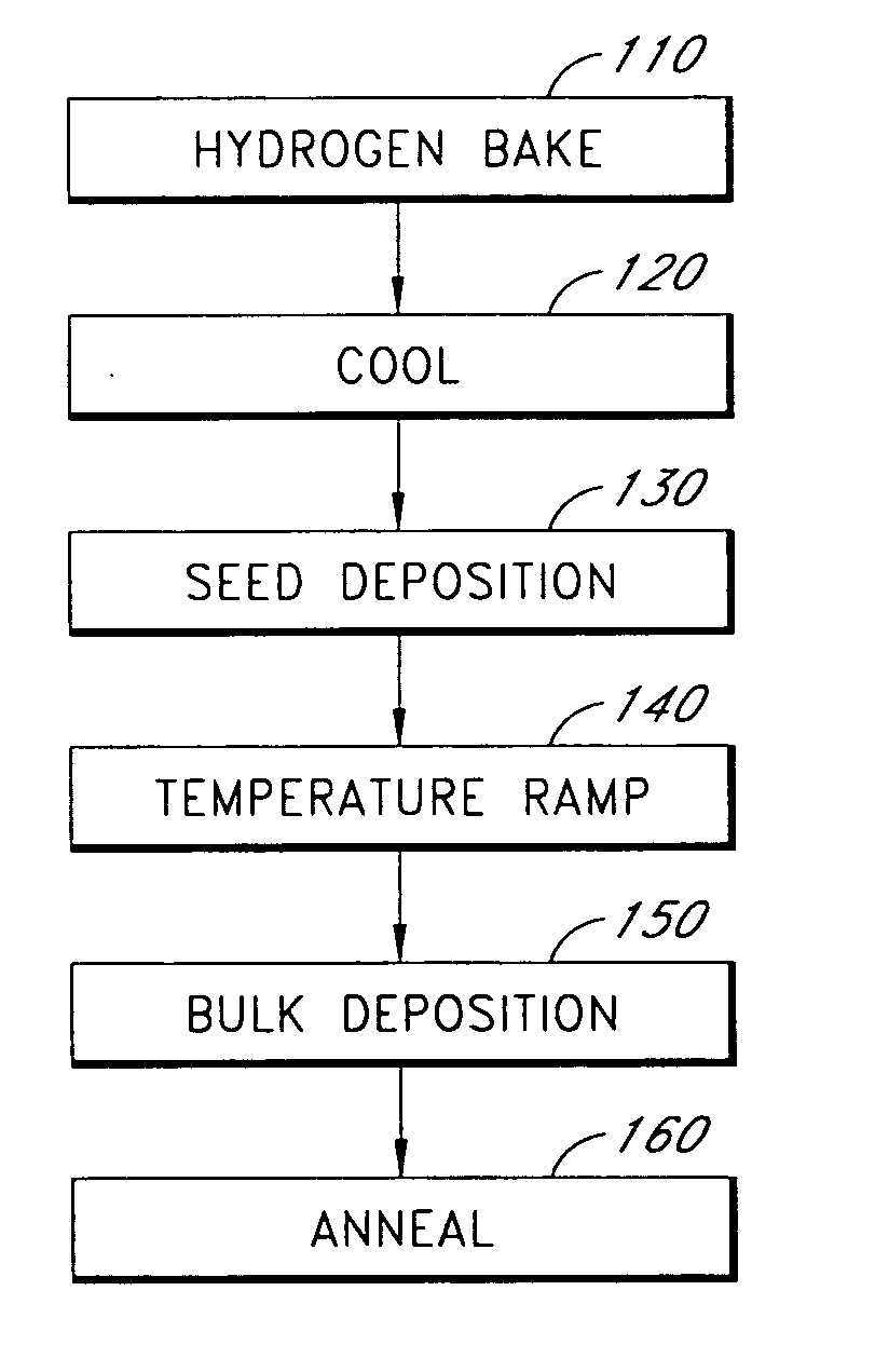
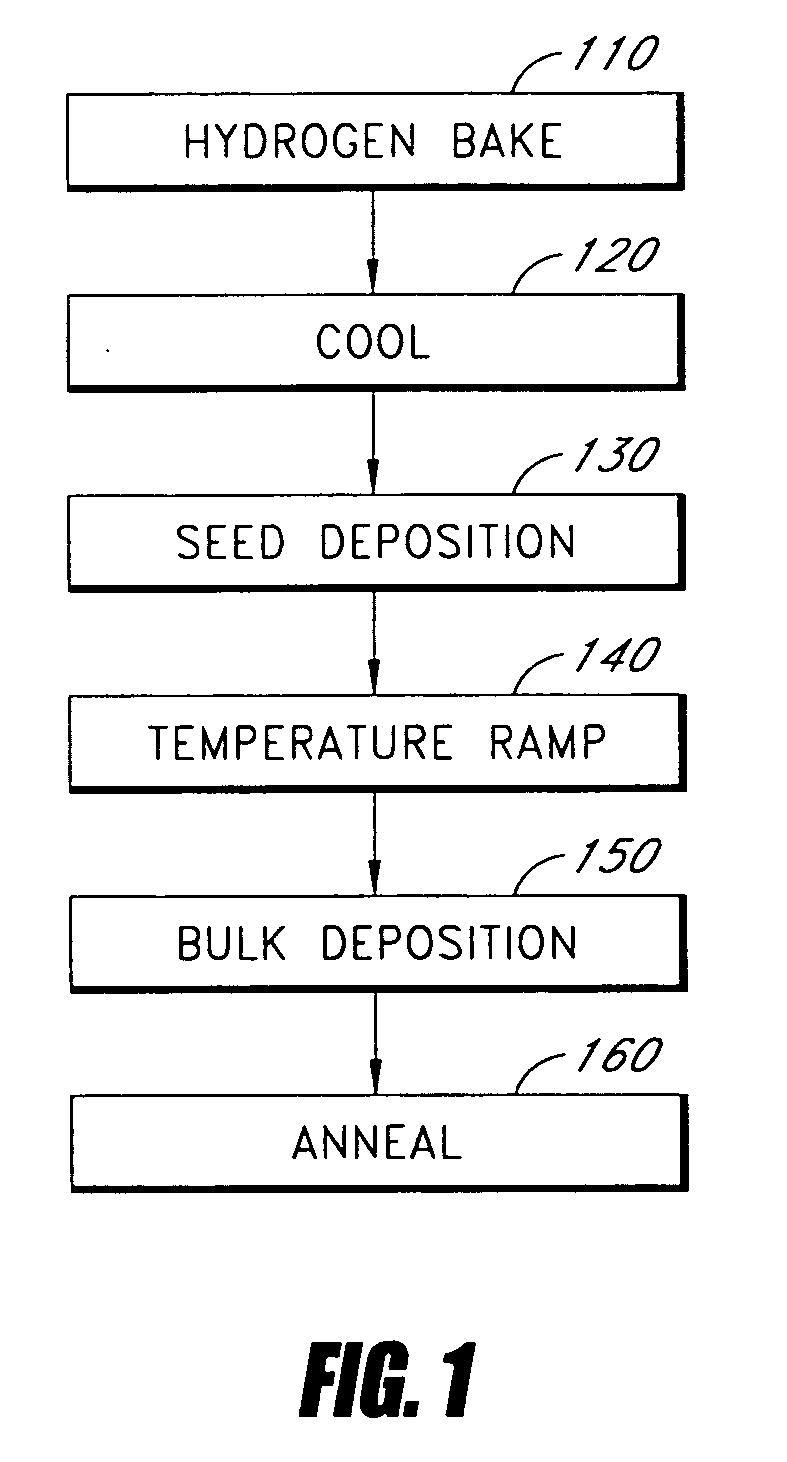
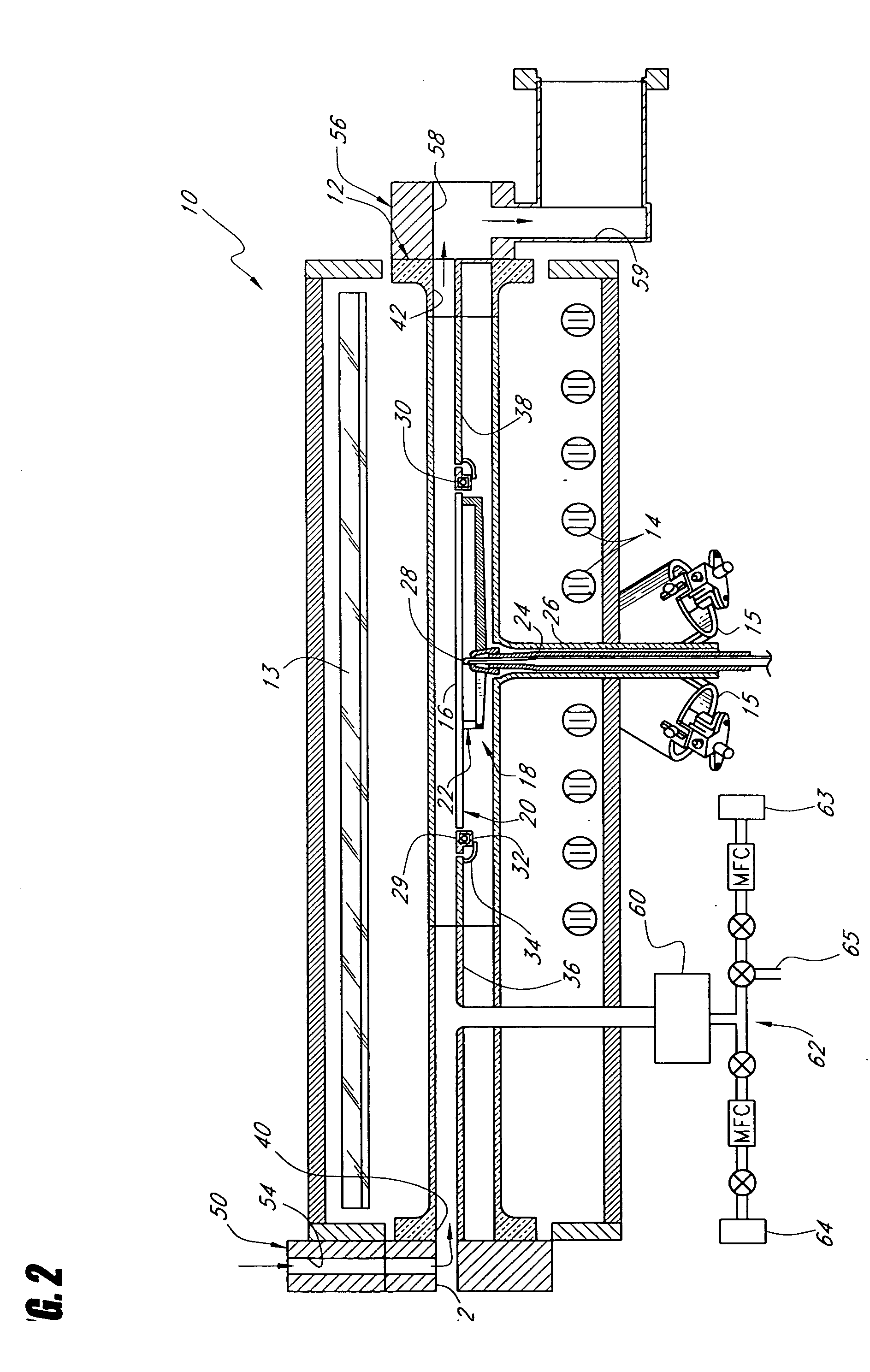
[0036] The disclosure provided herein describes several methods for depositing germanium films, including germanium films having improved physical characteristics, such as surface roughness and etch pit density. Germanium films offer a lower cost alternative to germanium substrates. Using certain of the methods described herein, germanium films are deposited using conventional CVD processing equipment. In particular, the deposition occurs in a sufficiently high pressure regime such that the use of UHVCVD is not required, and that better quality films are obtained. In certain embodiments, the germanium films are deposited over a silicon-containing surface, such as a silicon substrate. The term “substrate,” as used herein, refers to its ordinary meaning, as well as to a bare wafer or to such a workpiece with layers already formed thereon.

[0037] Although this disclosure refers to germanium films, and to illustrated embodiments and experiments conducted with “pure” germanium and doped ...


PUM


Abstract

A method comprises, in a reaction chamber, depositing a seed layer of germanium over a silicon-containing surface at a first temperature. The seed layer has a thickness between about one monolayer and about 1000 Å. The method further comprises, after depositing the seed layer, increasing the temperature of the reaction chamber while continuing to deposit germanium. The method further comprises holding the reaction chamber in a second temperature range while continuing to deposit germanium. The second temperature range is greater than the first temperature.

Description

PRIORITY APPLICATION [0001] This application claims the benefit of U.S. Provisional Patent Application 60 / 548,269 (filed 27 Feb. 2004) and U.S. Provisional Patent Application 60 / 556,752 (filed 26 Mar. 2004). The entire disclosure of these priority applications is hereby incorporated by reference herein.FIELD OF THE INVENTION [0002] This invention relates generally to methods for depositing germanium films, and relates more specifically to high quality heteroepitaxial germanium films that are formable using production-worthy chemical vapor deposition equipment. BACKGROUND OF THE INVENTION [0003] Germanium is used in a wide variety of applications, such as optoelectronics and quantum bit computing. For example, germanium is particularly useful in the manufacture of photodetectors, since conventional silicon photodetectors cannot detect the near-infrared light that is used for optical communications. Germanium films also advantageously offer good electrical carrier transport properties...

Claims


Application Information

Patent Timeline
Patent Type & Authority Applications(United States)
IPC IPC(8): H01L21/20H01L21/30H01L21/46
CPCC30B25/10C30B29/08C30B25/186C30B25/183Y10S438/935
Inventor BAUER, MATTHIABRABANT, PAULLANDIN, TREVAN
Owner ASM IP HLDG BV
Why Eureka
Try Eureka