Anisotropic conductive sheet and manufacture thereof

a technology of anisotropic conductivity and conductive sheet, which is applied in the manufacture of cables/conductors, dielectric characteristics, and conductors. it can solve the problems of fine metal wire buckles, difficult to maintain the anisotropic conductivity of a fine pitch required by modern high-integrated circuit boards, and difficult to reduce the distance between fine metal wires. achieve the effect of high productivity

Inactive Publication Date: 2005-09-08
JST MFG CO LTD
View PDF11 Cites 3 Cited by
  • Summary
  • Abstract
  • Description
  • Claims
  • Application Information

AI Technical Summary

Benefits of technology

[0069] The anisotropic conductive pieces include the conductive portions and the nonconductive portions that have uniform densities in a direction of the thickness, are suited for forming an anisotropic conductive sheet, and make it possible to obtain a so-called anisotropic conductive zebra sheet if the conductive portions are arranged in parallel. If the conductive portions are longitudinally and transversely arranged,

Problems solved by technology

With the anisotropic conductive sheet disclosed in JP-A-2000-340037 which uses fine metal wires, however, it is difficult to decrease the distance among the fine metal wires.
It is therefore difficult to maintain anisotropic conductivity of a fine pitch required by the modern highly integ

Method used


Image

  • Anisotropic conductive sheet and manufacture thereof
  • Anisotropic conductive sheet and manufacture thereof
  • Anisotropic conductive sheet and manufacture thereof

Examples


first embodiment

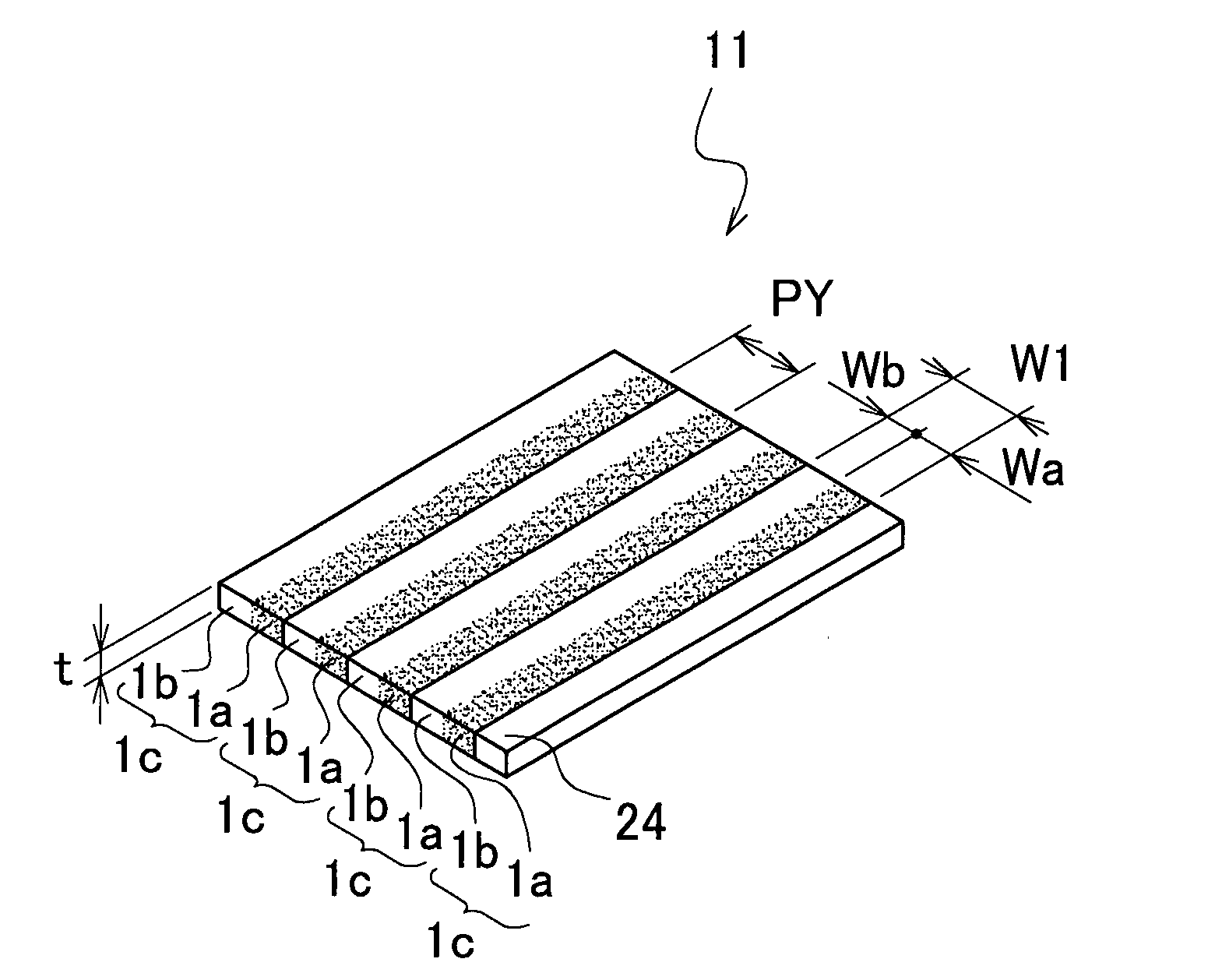
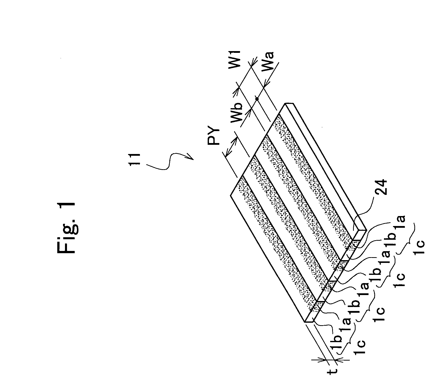
[0082] In the first embodiment in FIG. 1, a rectangular sheet member 1c includes a conductive portion 1a and a nonconductive portion integrally together, and forms an anisotropic conductive piece. The conductive portion 1a highly densely contains the conductive particles which are unevenly dispersed in a nonconductive elastomer having fluidity and serving as a matrix, the conductive particles having a specific gravity greater than that of the nonconductive matrix component. The nonconductive portion 1b is forming a substantially nonconductive portion since the conductive particles are unevenly dispersed in the nonconductive elastomer. Here, the conductive particles that are unevenly dispersed means that the conductive particles are unevenly dispersed in a direction of plane of the anisotropic conductive sheet 11 (direction nearly in parallel with the plane).

[0083] In the first form of the embodiment of FIG. 1, the sheet members 1c are arranged in line such that the conductive portio...

second embodiment

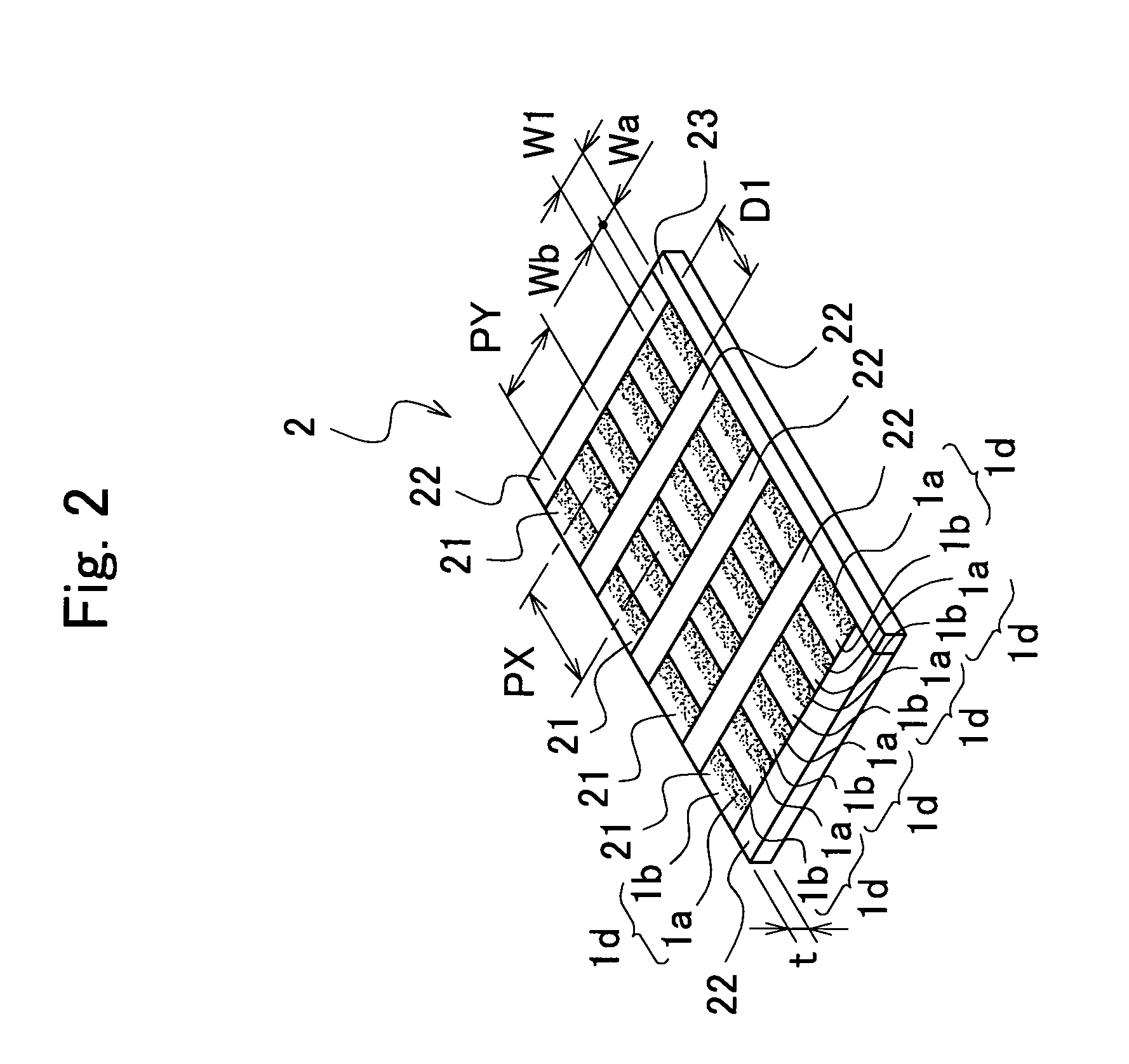
[0097] The anisotropic conductive sheet of the present invention uses, as the nonconductive elastomer, a silicone rubber manufactured by Mitsubishi Jushi Co. or a silicone rubber manufactured by Shin-etsu Polymer Co., and the coupling agent is a silane coupling agent manufactured by Shin-etsu Polymer Co.

[0098] Referring to FIG. 2, the anisotropic conductive sheet 2 includes the conductive portions 1a arranged like a matrix. The conductive portions 1a are forming through regions penetrating from the front surface to the back surface of the anisotropic conductive sheet 2. The sheet member 1d is forming the conductive portion 1a by mixing the conductive particles into the nonconductive matrix having fluidity in a manner that the conductive particles are unevenly dispersed by utilizing a difference in the specific gravity. The nonconductive portion 1b, on the other hand, is a separation layer formed by the unevenly dispersed conductive particles. The thus obtained anisotropic conductive...


PUM


Abstract

An anisotropic conductive sheet manufactured through improved manufacturing steps and a method of manufacturing the same. Conductive portions are unevenly arranged in a nonconductive elastomer having fluidity and serving as a matrix, the conductive portions highly densely containing the conductive particles having a specific gravity greater than that of the matrix component, the conductive particles are unevenly dispersed to form substantially nonconductive portions, and the conductive portions and the nonconductive portions are integrally cured to mold anisotropic conductive pieces. The anisotropic conductive pieces are so laminated that the conductive portions and the nonconductive portions are alternately arranged thereby to obtain a first laminate, and the first laminate is cut maintaining a predetermined thickness to obtain a zebra-like sheet. A second laminate obtained by alternately laminating the zebra-like sheets and the elastomer sheets is cut maintaining a predetermined thickness to obtain an isotropic conductive sheet in which the conductive portions are arranged like a matrix.

Description

CROSS-REFERENCE TO RELATED APPLICATIONS [0001] This application is based upon and claims the benefits of priority from Japanese Patent Application No. 2004-063155 filed on Mar. 5, 2004, the entire contents of which are incorporated herein by reference. FIELD OF THE INVENTION [0002] The present invention relates to an anisotropic conductive sheet, which may be interposed between a circuit board such as a printed board and various circuit parts, and to a method of manufacturing the same. RELATED ART [0003] The trend toward decreasing the size and thickness of modern electronic devices has required an increased necessity of connection among fine circuitry and among fine portions and fine circuitry. The method of connection is based on a solder junction technology and the use of an anisotropic conductive adhesive. There has further been employed a method of accomplishing electric conduction by interposing an anisotropic conductive elastomer sheet between the electronic part and the circ...

Claims


Application Information

Patent Timeline
IPC IPC(8): H01R11/01H01B5/16H01B13/00H01L21/48H01L21/60H01L23/48H05K3/32
CPCH05K3/325H05K2201/0133H05K2201/0314H05K2201/10378H05K2203/0235H01L2924/0002H01L2924/00013H01L2224/13099H01L2224/13599H01L2224/05599H01L2224/05099H01L2224/29099H01L2224/29599H01L2924/00
Inventor HASEGAWA, MIKI
Owner JST MFG CO LTD
Why Eureka
Try Eureka